JayKominek
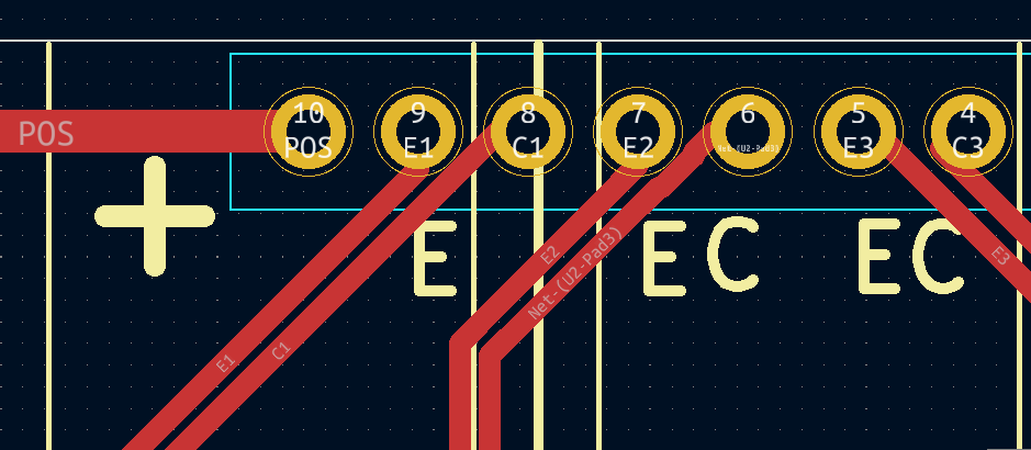
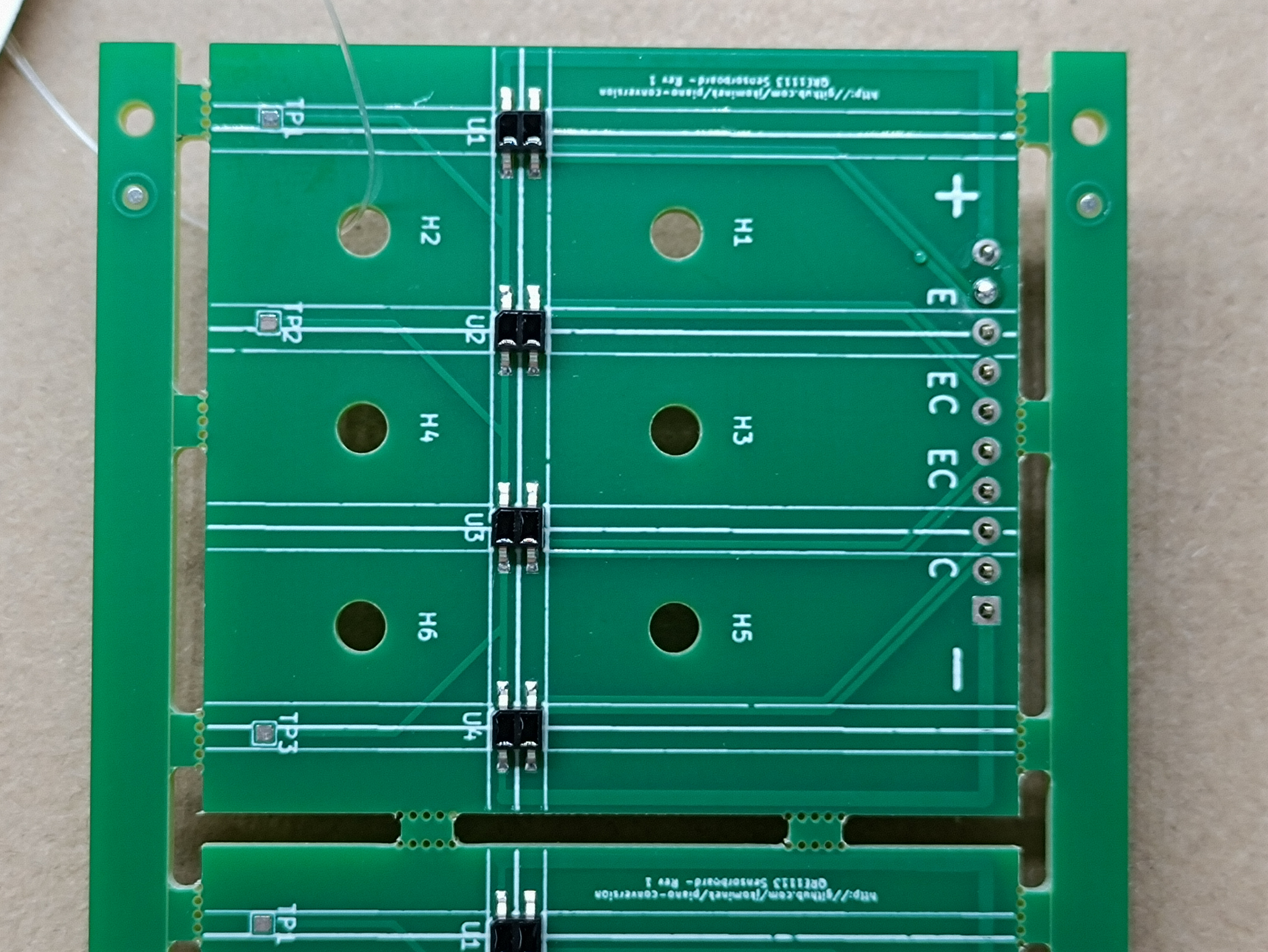
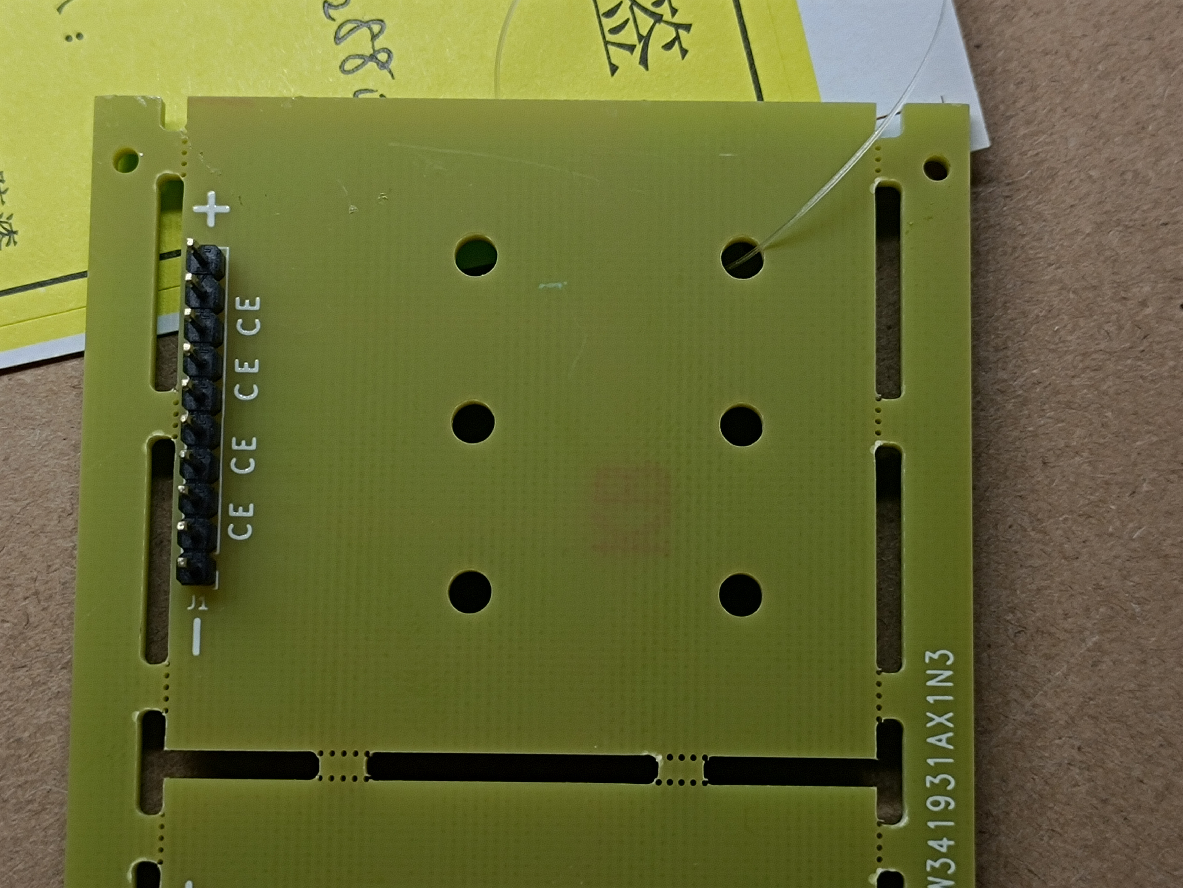
RIP The problem with that is that the soldering would be on the wrong side of the PCB, so the question for people who know more about that than I is if I could use the same mounting hole as a via, or if I need a separate via for that. As always, other solutions/ideas are well accepted and sought after.
"Mounting holes" aren't electrical, especially in Kicad. But the through holes used for through hole parts like pin headers are plated, just like vias. Things like pin headers can be soldered onto either side of the board, no problem. I do that on mine.
CyberGene My intuition tells me hammering the electronics directly is wrong. I can't explain why, maybe I'm wrong but I don't find that right, it will certainly stop working after a while.
The sensors themselves are potted in epoxy. Their failure is wildly unlikely. I'd expect the solder joints between them and the PCB to fail first. PCBs themselves have enough flex that I'd expect the traces to survive indefinitely.
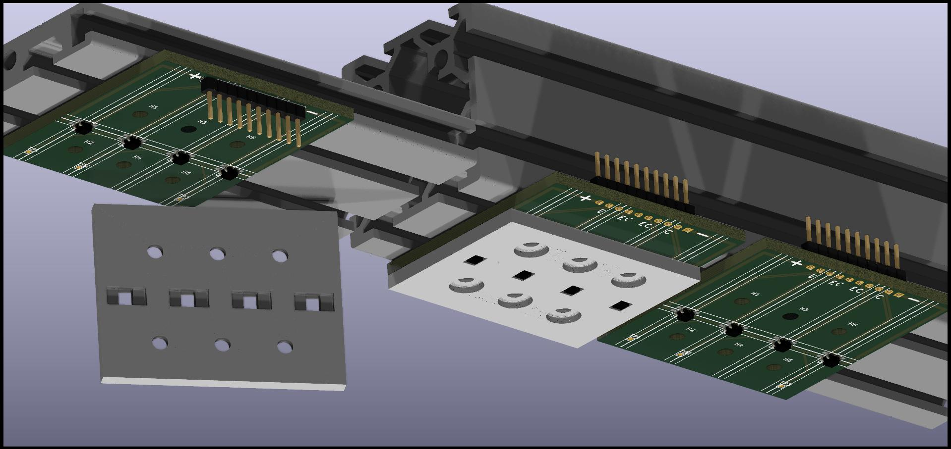
Personally I've got little 3D printed protector things, so that the hammers strike those (and are kept 2mm away from the sensor surface), and the force is distributed across the whole PCB. I then put some very thick electrical tape on the back side to cushion the interface between the PCB and the rail.
RIP Now, back to my question….
If you're going for automated / professional assembly, that's probably a question for the assembler.
If you're doing it by hand, then a very gentle press fit is probably ideal.
Solder will bridge the gap of any sane drill size, but it'll take a lot more solder (mostly a problem for hand assembly), and you increase the risk of parts falling out,