Skip to content

Update on piano conversion

RIP

Here is an update.

  1. are those 90 degrees bends ok on the power supply?
  2. I totally misread what you say and now I understand it. The one below is minimizing the bends to the minimum, but I think having one or two more bend per track to minimize distance will be better, do you agree?
  3. Done, lmk if I introduced other issues
  4. Done, lmk if I introduced other issues

If everything looks good (besides 2 which I am working on now) I'll update the PR accordingly (and for the 2x board too)

Thanks a lot once again!


RIP

Updated PR of 4x as discussed, here is my current proposal. Add some bends to the tracks, but I think the benefits of keeping them close outweights the cost.


scherbakov.​al

As a beginner in PCB manufacturing, I liked the easyeda.com editor. There is also automatic tracing and you can immediately order the manufacture of boards on jlcpcb.


RIP

scherbakov.​al As a beginner in PCB manufacturing, I liked the easyeda.com editor. There is also automatic tracing and you can immediately order the manufacture of boards on jlcpcb.

Does the automatic order submission and tracking include assembly or is it only for PCB manufacturing?

I've found that ordering PCB alone is tedious but doable, but I am yet to figure out what the various places want for ordering assembly…. which I definitely want because as Jay said "I'm sure as hell not tweaking 384 knobs" I say that I'm sure as hell not soldering 176 sensors, or even 176/4 boards since for SMT one can simply bake the board and solder 4 sensors at the time 😉

In any case, I am not making my own boards from zero here, but following the footprints of the giants, hoping to stand on their shoulders one day, so going "my way" (e.g. with EasyEDA) means that I won't be able to do that….


scherbakov.​al

RIP Does the automatic order submission and tracking include assembly or is it only for PCB manufacturing?

Yes, you can order boards with components installed on them. Their minimum order is 5 boards, 2 of which can be assembled with component placement. It is not expensive to place small surface details on the board. The installation of through components is expensive. I ordered boards and assemblies for several ICs and 2040 size resistors. Soldering such small parts in large quantities would have been extremely tedious and impossible in my current environment. But I soldered the optical sensors myself. I was very pleased with this service.


RIP

scherbakov.​al Yes, you can order boards with components installed on them.

Thanks! Maybe I'll give that a try, then. In fact, submitting JLCPCB requested assembly data via the regular webform is an exercise in frustration. We'll see if EasyEDA can cleanly import KiCad files.


RIP

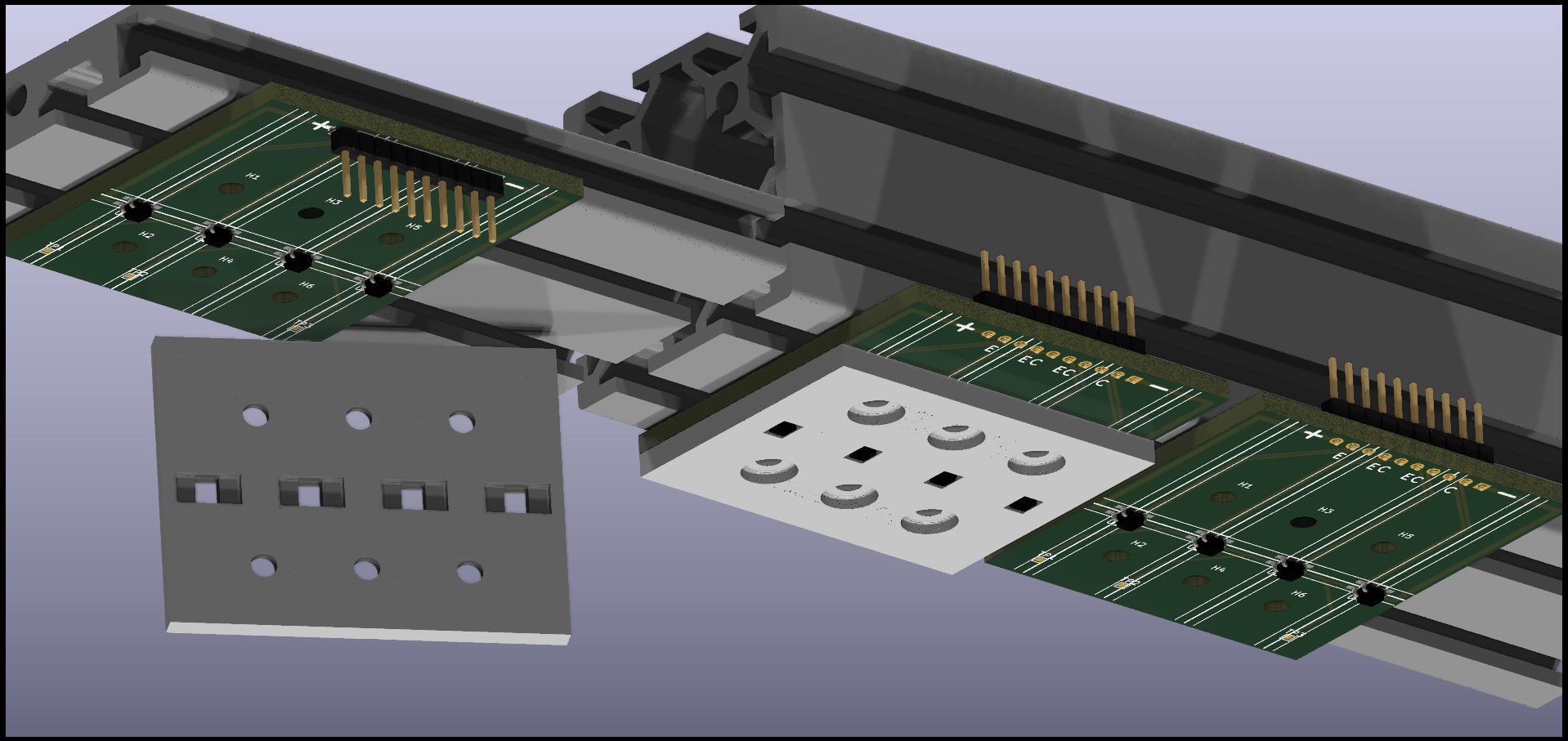
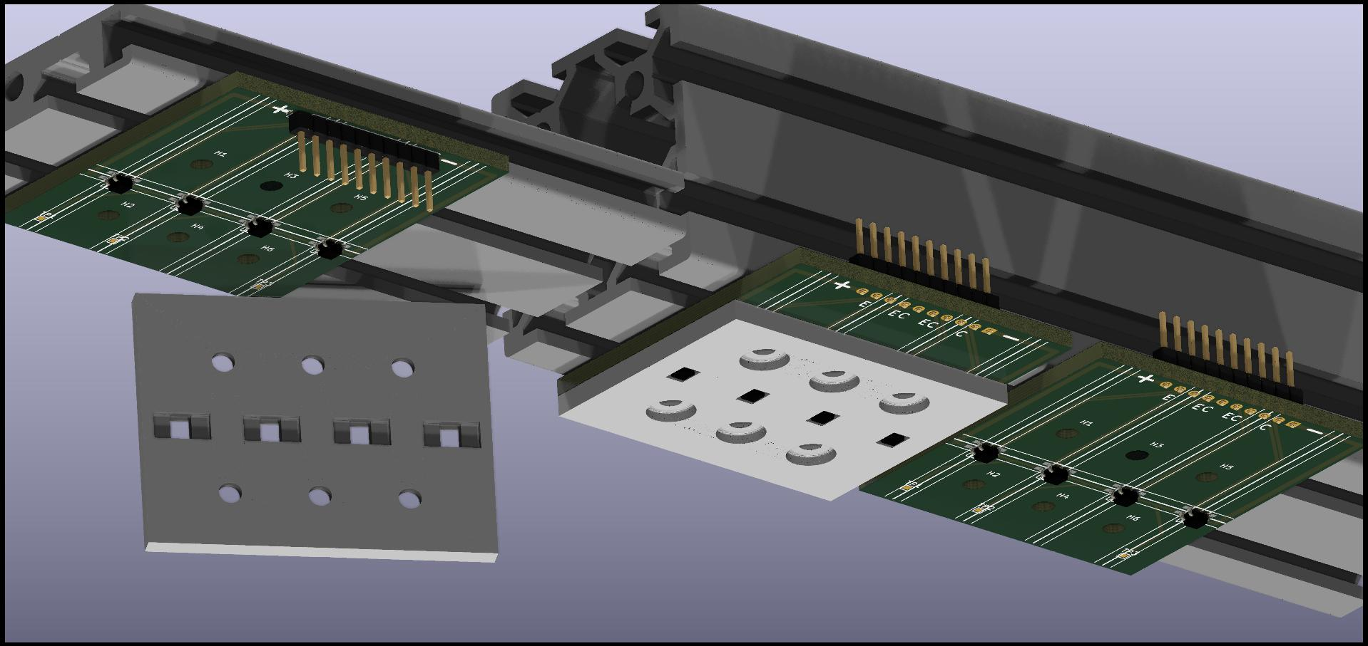
I've been silently working on and off on this, and I now have a question. For the hammer sensors, I am almost settled to the design mentioned above, which looks like this:

This works mechanically good, based on my cardboard models. In case it's not clear, you are looking at the sensors (those four black things on the green PCB) from the bottom. The hammers will hit them.

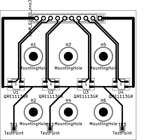
Now, for the damper sensors, the best approach would be to use a similar (note 1) board. The best way to mount that would be to use an extrusion like https://us.misumi-ec.com/vona2/detail/110302261730/?ProductCode=HFSQN4-1030-1382 to mount them under the keys, on the back where the back action is (or would be if it's removed). The problem is that header to attach the jumper connectors. It can't be in that direction, since that goes below the Keybed. One option could be to use angled connectors, but that has other complications that I don't want to get into, so my preference would be to simply mount the connector on the other side of the board, namely the same as where the sensors are.

The problem with that is that the soldering would be on the wrong side of the PCB, so the question for people who know more about that than I is if I could use the same mounting hole as a via, or if I need a separate via for that. As always, other solutions/ideas are well accepted and sought after.

(note1): since there is an extremely high cost for setup, having 176/4 + spare boards that are all identical would be most ideal, rather than 88/4 boards of one kind and 88/4 boards of another, which would cost more than double than having everything identical (I have already studied how to make sure that I can use boards with 4 sensors even though none of my hammer sections is made of a multiple of four hammers -- obviously there will be unused/unconnected sensors, the problem was that the spare one might be in the way).
I am not sure if the volume price would apply for an assembly of the jumper of two sides, but I hope so.


CyberGene

RIP The hammers will hit them

My intuition tells me hammering the electronics directly is wrong. I can't explain why, maybe I'm wrong but I don't find that right, it will certainly stop working after a while. Of course, you can experiment and prove me wrong 😀


JayKominek

RIP The problem with that is that the soldering would be on the wrong side of the PCB, so the question for people who know more about that than I is if I could use the same mounting hole as a via, or if I need a separate via for that. As always, other solutions/ideas are well accepted and sought after.

"Mounting holes" aren't electrical, especially in Kicad. But the through holes used for through hole parts like pin headers are plated, just like vias. Things like pin headers can be soldered onto either side of the board, no problem. I do that on mine.

CyberGene My intuition tells me hammering the electronics directly is wrong. I can't explain why, maybe I'm wrong but I don't find that right, it will certainly stop working after a while.

The sensors themselves are potted in epoxy. Their failure is wildly unlikely. I'd expect the solder joints between them and the PCB to fail first. PCBs themselves have enough flex that I'd expect the traces to survive indefinitely.

Personally I've got little 3D printed protector things, so that the hammers strike those (and are kept 2mm away from the sensor surface), and the force is distributed across the whole PCB. I then put some very thick electrical tape on the back side to cushion the interface between the PCB and the rail.

RIP Now, back to my question….

If you're going for automated / professional assembly, that's probably a question for the assembler.

If you're doing it by hand, then a very gentle press fit is probably ideal.

Solder will bridge the gap of any sane drill size, but it'll take a lot more solder (mostly a problem for hand assembly), and you increase the risk of parts falling out,


RIP

JayKominek "Mounting holes" aren't electrical, especially in Kicad. But the through holes used for through hole parts like pin headers are plated, just like vias. Things like pin headers can be soldered onto either side of the board, no problem.

Awesome.

JayKominek If you're going for automated / professional assembly, that's probably a question for the assembler.

Sounds great, I'll ask then.

JayKominek If you're doing it by hand, then a very gentle press fit is probably ideal.

Thanks a lot for the tips!


MacMacMac

CyberGene My intuition tells me hammering the electronics directly is wrong.

In my old Clav each key lever "hammers" upon its rubber contact.
And the rubber "hammers" upon the underlying PCB contacts.
Yes, they wear out eventually. But doesn't everything?


CyberGene

Digital piano actions are to a certain degree inconsistent in velocity detection because they rely on mechanical switches that will deteriorate from the constant banging. Optical contactless sensors can eliminate the wear. But if they are robust enough, they can take some beating.

I’d be also worried about vibrations in the rail causing neighboring sensors to oscillate longitudinally which can potentially reduce the precision of proximity detection but I guess that can be solved through using a very rigid rail that is fixed at multiple points.


RIP

CyberGene I’d be also worried about vibrations in the rail causing neighboring sensors to oscillate longitudinally which can potentially reduce the precision of proximity detection but I guess that can be solved through using a very rigid rail that is fixed at multiple points.

I was worried about that too. The flex computation from the specs did not help my "gut feeling". Holding that aluminum extrusion which you can see on the rendering I posted earlier today, did. That extrusion is really, really rigid. If you think the flex computation can help, the specs are on the misumi website.

CyberGene But if they are robust enough, they can take some beating.

JayKominek Personally I've got little 3D printed protector things, so that the hammers strike those

I could do the same thing Jay did, which you can see at https://github.com/jkominek/piano-conversion/tree/master/mechanical (I thought I saw a picture once, but can't find it right now). With the smaller sensors will actually be much easier to align and more effective since the "hole" would be much smaller and protective. I have just too many balls to juggle at the moment, but if anybody is interested in this design, and could do the 3D model for that, it'd be a nice plus. But it's just a plus, I'm confident it'll get years of service even without. The perfect is the enemy of the good, and if I try to do everything perfectly, I'll end up never finishing (which some days already feels like it)


RIP

RIP CyberGene But if they are robust enough, they can take some beating.

JayKominek Personally I've got little 3D printed protector things, so that the hammers strike those

I could do the same thing Jay did

And now I did (not 3D printed yet). Getting started was really tough, (see the commit messages for details). 3D manufacturing is not that easy, unless you can use just one product.

I also oh-so-slightly modified the board as follows:

  • made it slightly longer, to be easier to attach to thinner extrusions (which happen to be larger, go figure MISUMI) for use as a key sensor
  • being longer, I've been able to avoid one other bend in the trace of the sensors to the connector
  • added silkscreen reference lines to aid alignment, especially for the key sensors which may not be super-accessible in all circumstances

And TADA 🎉 here is the result.

See description of what you are seeing at

https://github.com/davidedelvento/piano-conversion/tree/master/hardware/sensorboards/2040-centered-4x-QRE1113GR/ (not sure how to embed the README.md from github to here, sigh, it wants to show only by ugly face of more than a decade ago….)

I need to sleep on it, and hope that both @"CyberGene" and @"JayKominek" (and possibly others) give a look at both the latest revision of the board and of the protector, and now I am really ready to order both. I plan to do it at https://www.pcbway.com/ which I like better than JLCPCB and 4PCB: one-stop-shopping (even 3D printing, so one order for everything) and especially a decent submit form rather than the unusable cr** [1] the other two offer.

[1]: for a newbie like myself, their staying in business implies that other people, likely experts, don't cry as much as I do when using them


CyberGene

How are you going to attach the plastic coverings to the PCB? Plastic may cause a lot of clacking noises if large enough and hit by a hammer.


RIP

CyberGene How are you going to attach the plastic coverings to the PCB?

Yes. As almost everything else, Jay had the initial idea, so if it's a good one, it's his, but if it isn't working, I designed it myself, so it's my fault 😐

Plastic may cause a lot of clacking noises if large enough and hit by a hammer.

You are never satisfied, @CyberGene are you? 🙂
You are probably spending too much time with @porco_rosso these days 🤣 (no offense intended Eddie, if anything that is actually a compliment for being a perfectionist -- as I am in fact myself)

I thought of that already. If necessary I can and will use thin fabric/felt stuff (already have lots of samples) in between

  • metal and PCB (in the bass),
  • metal and plastic spacer (in the treble, to correct for the different height due to overstringing)
  • plastic spacer and PCB (ditto)
  • PCB and plastic protector (the thing you are talking about)
  • and even plastic protector and the hammer

In theory you could do digital analysis of these noises, but that's really above and beyond what I am willing to make. Instead, trial and error should be manageable enough (besides that the necessary thickness of the ones mentioned in the last two bullet points might make the sensors buried "too deeply" inside, but I doubt we'll reach that point -- the other ones can be as thick as I want and easy to adjust for given the extrusion attachment design I have).

Now, for something which I have only done in a cursory way, please go check if my tolerances are enough for the manufacturing/assembly process while still not leaving too big of a gap for the hammers to be caught into 😃

Plastic spacer mentioned above:

https://www.amazon.com/gp/product/B01LXGL3HG/


CyberGene

I just had to say something 😀 My way of thinking is always about seeking for what may go wrong, apologies if it sounds like I’m critical. Ask my wife, she will complain about me always thinking only about the negative outcomes of everything 🤣

Other than that it looks like you’re making great progress and you said you were gonna freeze it, so that’s even more good news that you managed to find time to work on that project! I’m looking forward to the final result.

As to PCB, I don’t feel I’m competent enough to comment on that since what I did on Cybrid was probably very amateurish and I haven’t read or researched anything about good PCB design. My understanding is that’s not very important unless you create very high-frequency schematics and/or analog type of electronics. But I might be wrong.


RIP

CyberGene apologies if it sounds like I’m critical.

You don't. That's the right way to do the design if you want to have a minimal chance to succeed.

CyberGene Ask my wife

Too bad we leave so far, you and I would be best friends, and our wives too 🤣

CyberGene As to PCB, I don’t feel I’m competent enough to comment on that since what I did on Cybrid was probably very amateurish

The comments I was looking for are very basics: KiCad does not give errors (but gives too many warnings because it does not like the way I made the silkscreen-over-other-things-including-itself). But are the default minima ok? Am I coming too close to the adjacent jumper connector since I arrive at 45 degrees to reduce the number of turns? Very simple things like that, both these listed here and other I might not have thought about. But I was asking that part to mostly Jay. For you, @CyberGene I was thinking of the sensor protector, since I banged my head on the keyboard too much [1] to trust myself that I got it right. If the holes are in the wrong spot, I'm just getting shipped a bunch of just plastic from China….

[1]: See here


RIP

Forgot to mention:

  1. their price structure is not "raw", which I like. With the others, ordering one board or two costed the same money. Ordering 10 or 20 (or any doubling up to thousands) costed 5-10%. I totally get why, but that put psychological pressure on finding asap lots of people interested in the project and order together. With these, even with the volume discount which is there, the price is not so massively biased toward huge numbers. As such, I can order what I need for myself, plenty of spares (but not a full second instrument) and be content. If anybody wants to order theirs….
  2. they offer a one-click option in which if I want I can make my project available for others to order. So, once I'm settled, I don't have to explain on github what to do and how, I can just say "click here, pay and the correct parts will show up at your door". Given how painful it's been exploring the other two PCB manufacturing and assembly companies, for me this is a huge plus.

« Previous Page Next Page »