![]()
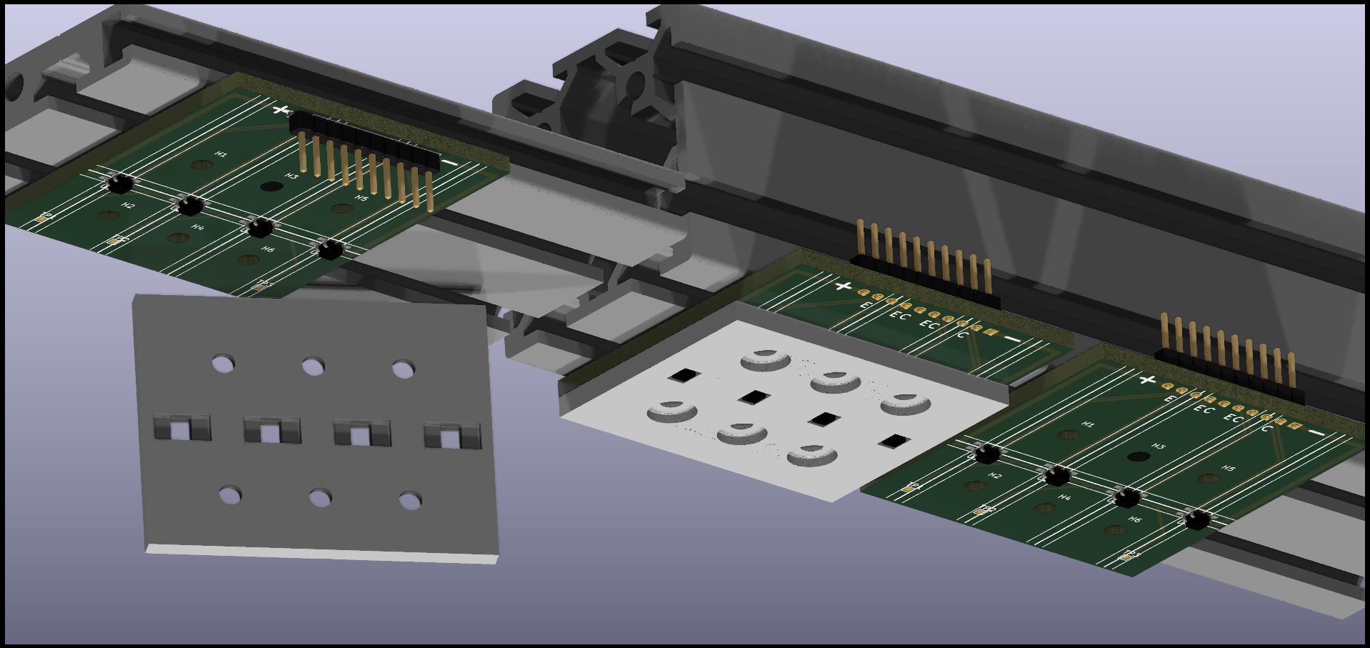
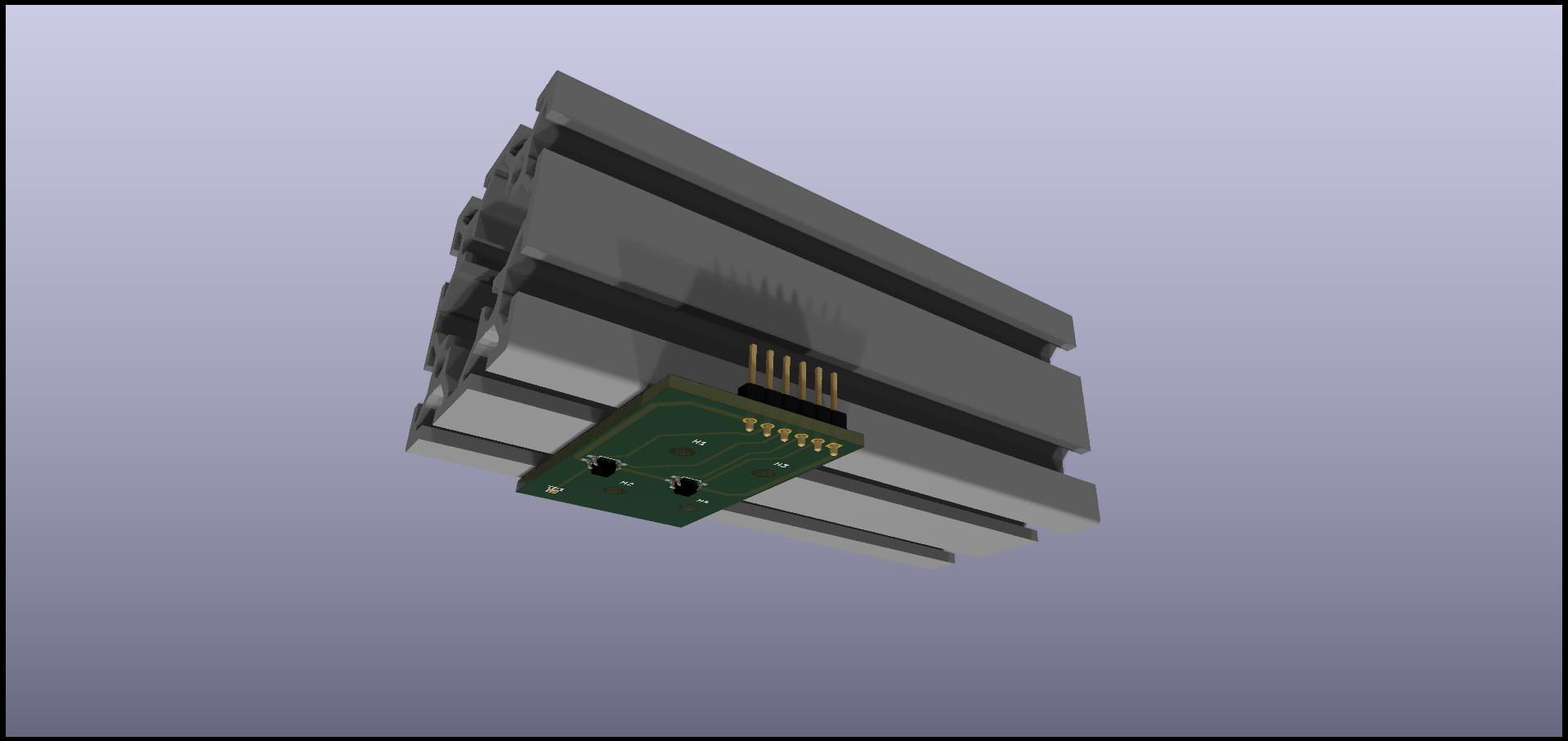
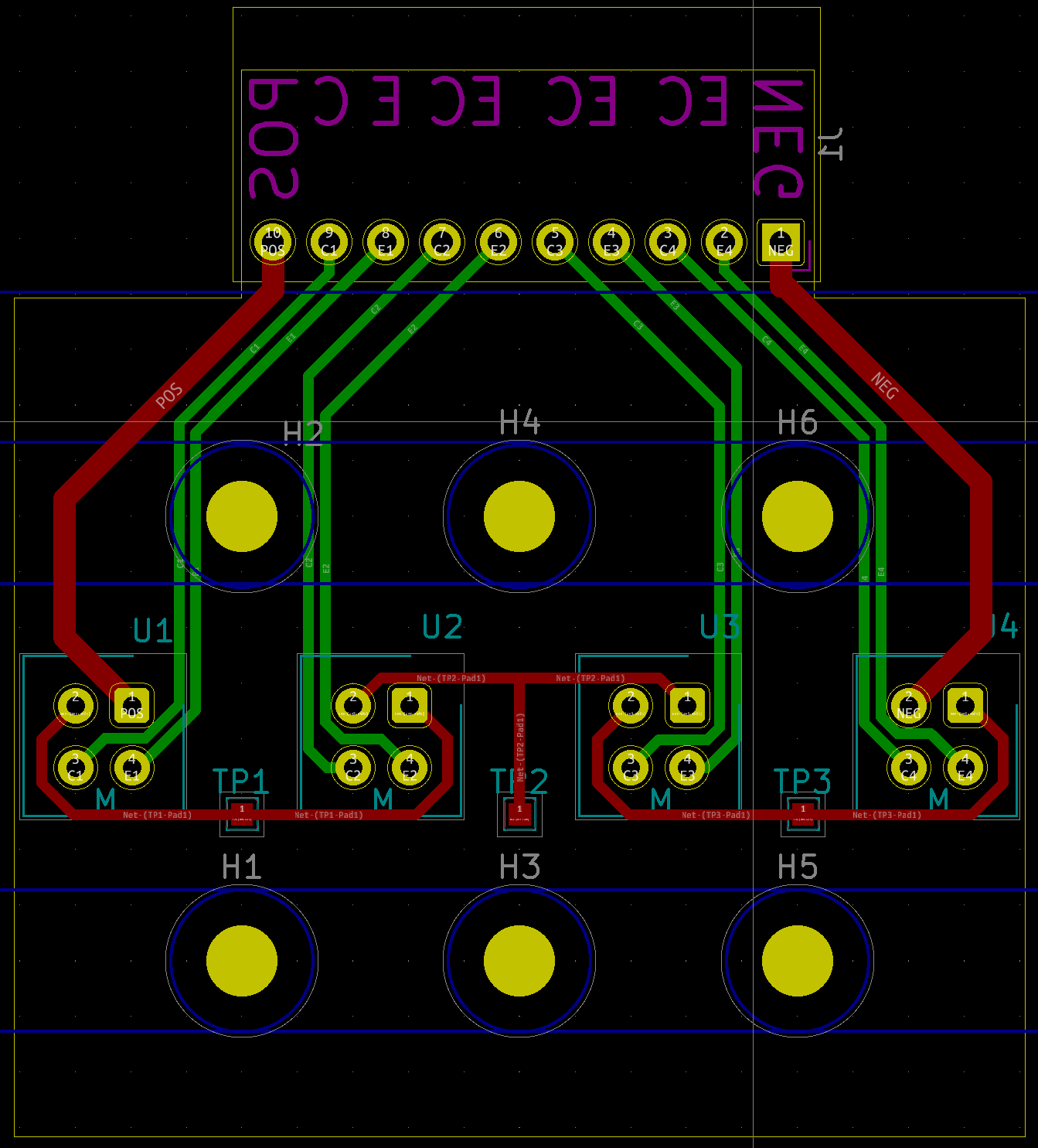
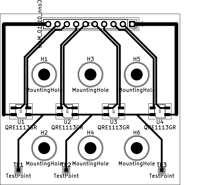
Since there was some, uh, general interest in PCB layout above, I'll comment here. I'm using the 4x sensor board as an example, but the same issues were present on the 2x board.
I didn't check pinouts very hard, but assuming they're right, the board should work fine.
Reiterating: board should work fine.
Layout could be better, for free, though. Nit-picking commences:
- You've got unnecessary bends in the traces. Every change in width (which a bend causes) represents a change in impedance, which causes reflections, potentially EMI, etc.
- The pairs of traces with those screw holes going through them represent current loops. The bigger the space between them, the more noise they can pick up, and the more they can generate. The trace pairs should run as close as possible. (For carrying the signal from these boards back to the ADC board, I specify twisted pair, to ensure that space is minimized.)
- I try (weakly) to avoid entering pads diagonally. It increases the width of the connection between the pad and the trace, which makes it easier for the pad to lose heat to the trace during the soldering process. Sometimes it is unavoidable. This isn't one of those situations.
- Those thick traces entering tiny pads will make them more difficult to solder, as the traces can soak up the heat. Also, the test points meeting up with the net at the pad is unnecessary; the voltage will be the same in the middle of the trace between Ux and U(x+1) as it is at either end. By moving it to the middle, you reduce heat lost to that trace.
Apropos of the autorouter discussion, for it to be good at laying out something as simple as this board, you'd need it to know:
- That the power nets are power nets,
- and that they're driven by a constant current driver, so their twisty windiness doesn't matter.
- It would also be helpful for it to know that the power supply actually has quite a lot of voltage overhead, and so thickening the traces to reduce losses is only bonus points.
- It should also know that the signal traces come in pairs, and form part of a current loop.
- Last, it would need to know that the test points are for taking voltage measurements, and will carry no current, so they should be moved away from pads to ease manufacturing, and can have thin traces.
(I'm not aware of ever having worked on, or seen, a board which was laid out with an autorouter.)
(But Jay, some of your early boards didn't do things you said to do above! Yeah, I've gotten a lot of layout practice on this project, and spent a bunch of time reading Electromagnetic Compatibility Engineering.)