Skip to content

Update on piano conversion

RIP

So I did find some time to play with KiCad in the last week with family out of town (between a decent running fall which scarred half my face, a sewer backup, a check lost in the mail, and other minor hiccups). So much so that I created https://github.com/jkominek/piano-conversion/pull/53

I think my problem with KiCad was that I was thinking of it as a smart tool that could help with all sorts of decisions, whereas the right approach is thinking of it like dumb paper-and-pencil thing (like in the good ole day of acid etching which I always wanted to do as a teen but never got permissions from my parents). With that attitude, I've been able to make some progress, rather than spend hours searching for "where's the feature to do X?" only to find out that there isn't and you have to do it manually.


CyberGene

RIP decent running fall which scarred half my face

Sorry to hear that, I hope you’re getting well.

I used KiCad only to prepare my PCB-s and was glad I was over with it and wouldn’t have to use it ever again 😀 Had to Google on every step. OTOH I can certainly say I (it?) did extremely well in that regard. Taking in mind it’s free, there’s not much to complain about.


RIP

CyberGene Del Vento decent running fall which scarred half my face

Sorry to hear that, I hope you’re getting well.

Thank you! I'm recovering well, just some bruises and scabs remain. Luckily, no bones (or teeth!!) damaged.

I used KiCad only to prepare my PCB-s and was glad it was over 😀 Had to Google on every step. OTOH I can certainly say I (it?) dit extremely well in that regard. Taking in mind it’s free, there’s not much to complain about.

It was just that I had too high expectations, for example I expected by default creating the track routes (to be modified by hand only if necessary). Instead it gives the radsnet and the user has to manually route connection-by-connection (and then make sure don't move components, or if you do you, you have move the tracks too….)

As you say, it's a great tool -- but only after I reached to it with a paper-and-pencil attitude, which do nothing about what you are drawing with them -- rather than expecting it to automatically do "the right thing" knowing all about the intended context (admittedly KiCad is much better than paper-and-pencil, but not as automated as it could be)


CyberGene

RIP for example I expected by default creating the track routes (to be modified by hand only if necessary)

Yeah, that was disappointing but I think on their website they pointed to a free Java program that could make auto-routing, you keep it running for as long as possible and it would come up with a pretty good routing. I ended up with a hybrid approach where I created some routes myself (those around connectors that followed certain symmetry and then left out the rest to the auto-router and I think the final result was pretty good.


RIP

CyberGene Yeah, that was disappointing but I think on their website they pointed to a free Java program that could make auto-routing

Ah, I missed that. Interesting, I wonder why they did not make that a part of KiCad itself instead… Not a big deal in my case, but probably a big deal for larger projects.

Pinging @JayKominek and @vagfilm who I initially didn't since I thought most of the conversation happening on github.


CyberGene

RIP BTW, the Java program was long ago abandoned, so I built it from sources and had to fix a few trivial things to be able to compile it under Java 8. So, it’s all pretty awkward… But other than that it’s a fantastic program! You should definitely give it a try.


CyberGene

And while calculating you see visually the routes changing. It will first come up with a solution (usually with a lot of vias) but if you keep it running longer it starts optimizing it and minimizing the vias, etc. I could watch it hypnotized for hours 😀


RIP

CyberGene And while calculating you see visually the routes changing.

Wow, really cool. I'll check it out. Thanks for pointing it out!

CyberGene BTW, the Java program was long ago abandoned, so I built it from sources and had to fix a few trivial things to be able to compile it under Java 8.

Not a problem, java's easy to deal with.


RIP

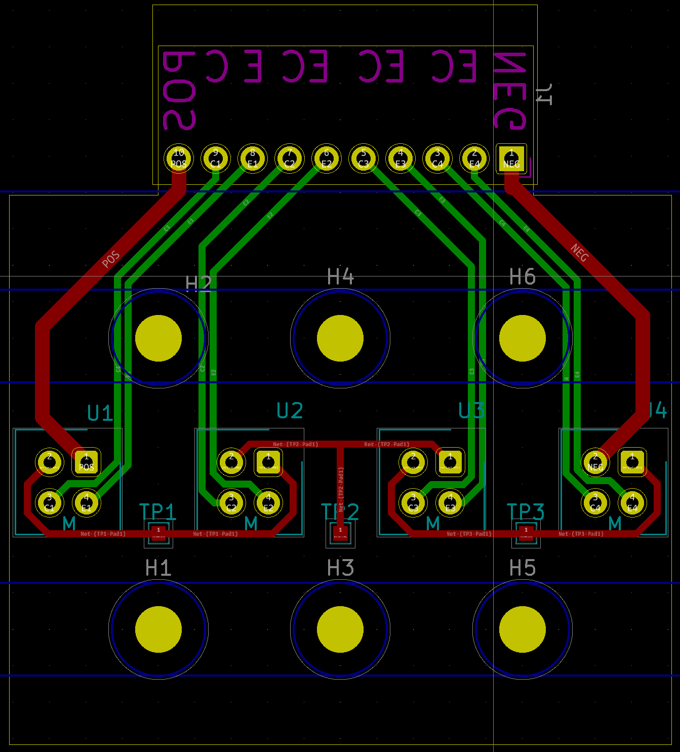
In case anybody wants to take a peek, I update the PR and opened another one.


RIP

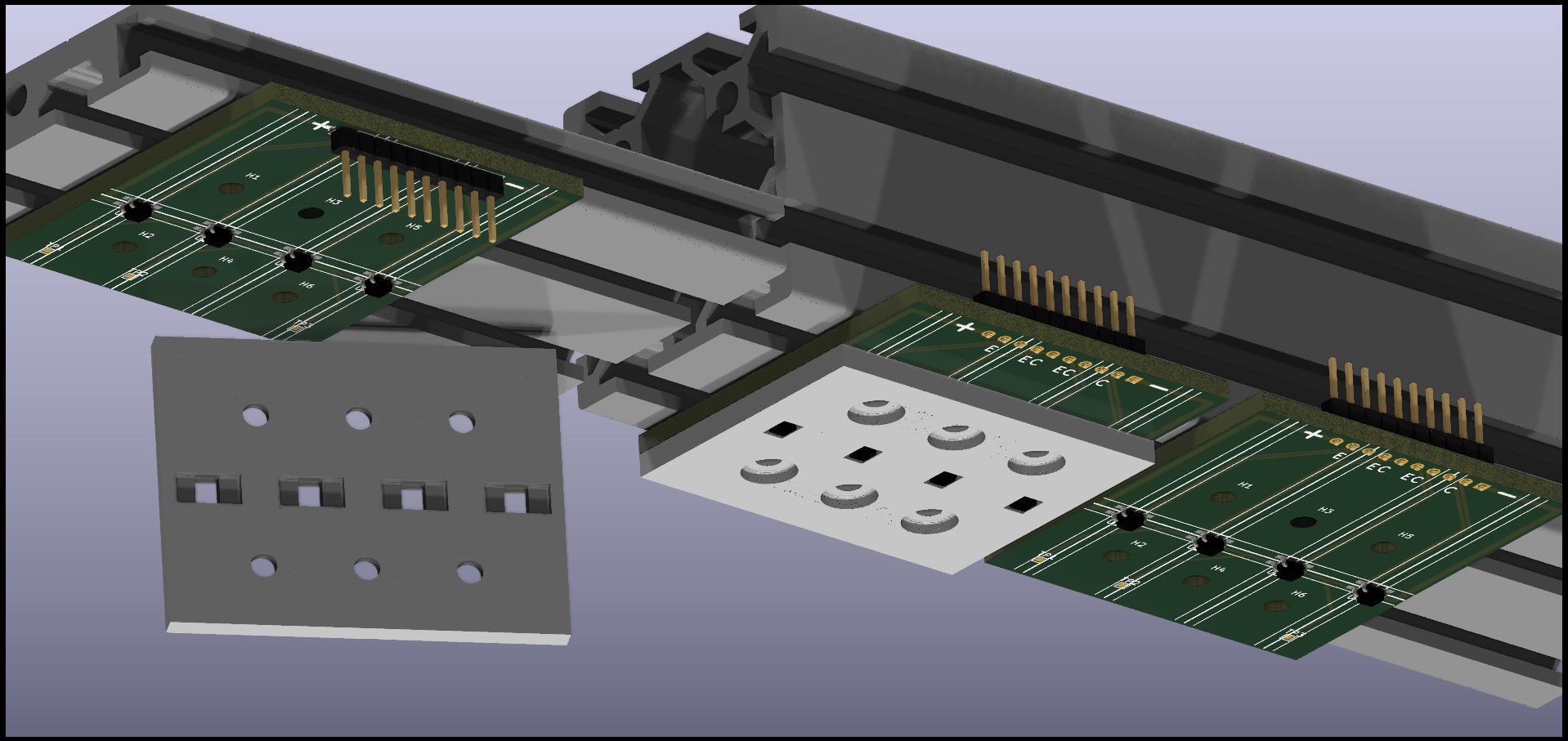
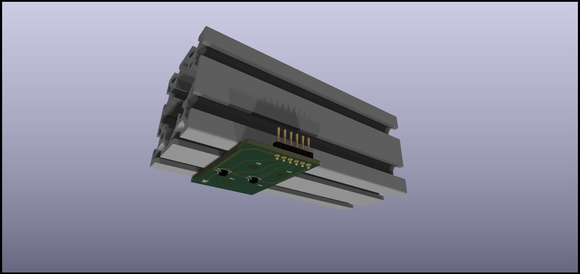
I see, to pique the interest of the clique so people make an appropriate piano clack, you guys need a few thousands of words, aka pictures. Here you are!

things explained here for the previous one and

things explained here for the last picture (link different from the other one!)

@JayKominek if you can find the time to give even a cursory look at these boards (you might want to use the PRs) I'd greatly appreciate that. I suspect I may have made some glaring mistake and I'd love to learn before making an order, which I hope to make this week. I think I am done fiddling with them. Thanks!!


RIP

If any of you want to have some stubs in your hands, print the following pages (make sure you are really printing at 100% for example checking that your 4x boards are 49mm x 47mm) and then cut them with scissors.

2x-panel.pdf
117kB
4x-panel.pdf
197kB

(if there's interest I can push these to github which seemed unnecessary clutter)

EDIT: These two files got inadvertently deleted as described at https://pianoclack.com/forum/d/1222-i-have-inadvertently-deleted-some-files-on-the-forum/17 and I am not spending the time to re-upload it unless someone asks


JayKominek

Since there was some, uh, general interest in PCB layout above, I'll comment here. I'm using the 4x sensor board as an example, but the same issues were present on the 2x board.

I didn't check pinouts very hard, but assuming they're right, the board should work fine.

Reiterating: board should work fine.

Layout could be better, for free, though. Nit-picking commences:

  1. You've got unnecessary bends in the traces. Every change in width (which a bend causes) represents a change in impedance, which causes reflections, potentially EMI, etc.
  2. The pairs of traces with those screw holes going through them represent current loops. The bigger the space between them, the more noise they can pick up, and the more they can generate. The trace pairs should run as close as possible. (For carrying the signal from these boards back to the ADC board, I specify twisted pair, to ensure that space is minimized.)
  3. I try (weakly) to avoid entering pads diagonally. It increases the width of the connection between the pad and the trace, which makes it easier for the pad to lose heat to the trace during the soldering process. Sometimes it is unavoidable. This isn't one of those situations.
  4. Those thick traces entering tiny pads will make them more difficult to solder, as the traces can soak up the heat. Also, the test points meeting up with the net at the pad is unnecessary; the voltage will be the same in the middle of the trace between Ux and U(x+1) as it is at either end. By moving it to the middle, you reduce heat lost to that trace.

Apropos of the autorouter discussion, for it to be good at laying out something as simple as this board, you'd need it to know:

  1. That the power nets are power nets,
  2. and that they're driven by a constant current driver, so their twisty windiness doesn't matter.
  3. It would also be helpful for it to know that the power supply actually has quite a lot of voltage overhead, and so thickening the traces to reduce losses is only bonus points.
  4. It should also know that the signal traces come in pairs, and form part of a current loop.
  5. Last, it would need to know that the test points are for taking voltage measurements, and will carry no current, so they should be moved away from pads to ease manufacturing, and can have thin traces.

(I'm not aware of ever having worked on, or seen, a board which was laid out with an autorouter.)

(But Jay, some of your early boards didn't do things you said to do above! Yeah, I've gotten a lot of layout practice on this project, and spent a bunch of time reading Electromagnetic Compatibility Engineering.)

RIP

JayKominek

Awesome thanks a lot for this feedbac! Obviously I knew close to nothing about the best ways to make the board easier to solder. Some comments and one follow up question

  1. I'll remove them. Some of them (e.g. the one on the right in this picture) I made on purpose to keep more distance from the power supply. Some others (second pin of the connector from the left) I made it because I was still fighting with how to use KiCad GUI and then it stayed that way.
  2. I am not sure I understand this: aren't they close enough? Moreover, I copied them from the holes in your other sensorboards, did I screw up the copy paste or do they have the same issue?
  3. I was not aware of this issue, thanks
  4. So you'd reduce the track width just before entering the pads? I'll move the test point traces.

JayKominek

RIP

  1. Generally not a bad plan to keep the signals away from the power, but these power traces shouldn't be generating (much? any?) noise, compared to what you'd see attaching a switch mode power supply to a microcontroller, or similar. It's a linear supply feeding LEDs. The only variation will be from the LEDs aging, or the temperature in the room changing.
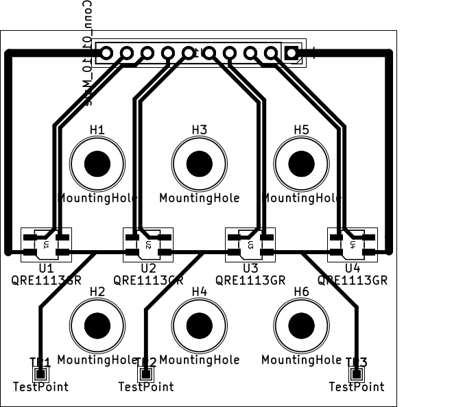
  2. The trace pairs should be as close as manufacturing tolerances allow. I think I failed to do that on one of my early layouts. I've attached a screenshot of what the current layout looks.
  3. 👍
  4. I'd at least consider doing exactly that. (Or just don't worry about making them thicker. It just means you'll dissipate some of the waste voltage in those traces instead of in the MOSFET on the LED power board.) With solid ground pours, you've got to do it (it is called "thermal relief", if you look in the configuration options for a ground plane in Kicad), with thick traces, there's no automatic mechanism. If you look on my ADC or LED board layouts, I think I've got some spots where I bring thick power traces to a regulator, or diode or something, and narrow it down right at the last moment. Generally because I had difficulty hand soldering that exact spot in one of my early revs.

There aren't any surface mount pads that count on this one, I kept the signal traces (which all happen to be green) extremely close on this one, without adding any unnecessary bends. (They could be slightly closer for U2 and U3, both at the top and the bottom, but, ehhh.) I do add some space between power and signal, beyond the fact that they're on separate layers, but I do it by adding the wiggling to the power traces. I do enter some of those square through hole pads diagonally, but they're already getting waaaay more heat and solder than an SMT pad ever would.


RIP

Here is an update.

  1. are those 90 degrees bends ok on the power supply?
  2. I totally misread what you say and now I understand it. The one below is minimizing the bends to the minimum, but I think having one or two more bend per track to minimize distance will be better, do you agree?
  3. Done, lmk if I introduced other issues
  4. Done, lmk if I introduced other issues

If everything looks good (besides 2 which I am working on now) I'll update the PR accordingly (and for the 2x board too)

Thanks a lot once again!


RIP

Updated PR of 4x as discussed, here is my current proposal. Add some bends to the tracks, but I think the benefits of keeping them close outweights the cost.


scherbakov.​al

As a beginner in PCB manufacturing, I liked the easyeda.com editor. There is also automatic tracing and you can immediately order the manufacture of boards on jlcpcb.


RIP

scherbakov.​al As a beginner in PCB manufacturing, I liked the easyeda.com editor. There is also automatic tracing and you can immediately order the manufacture of boards on jlcpcb.

Does the automatic order submission and tracking include assembly or is it only for PCB manufacturing?

I've found that ordering PCB alone is tedious but doable, but I am yet to figure out what the various places want for ordering assembly…. which I definitely want because as Jay said "I'm sure as hell not tweaking 384 knobs" I say that I'm sure as hell not soldering 176 sensors, or even 176/4 boards since for SMT one can simply bake the board and solder 4 sensors at the time 😉

In any case, I am not making my own boards from zero here, but following the footprints of the giants, hoping to stand on their shoulders one day, so going "my way" (e.g. with EasyEDA) means that I won't be able to do that….


scherbakov.​al

RIP Does the automatic order submission and tracking include assembly or is it only for PCB manufacturing?

Yes, you can order boards with components installed on them. Their minimum order is 5 boards, 2 of which can be assembled with component placement. It is not expensive to place small surface details on the board. The installation of through components is expensive. I ordered boards and assemblies for several ICs and 2040 size resistors. Soldering such small parts in large quantities would have been extremely tedious and impossible in my current environment. But I soldered the optical sensors myself. I was very pleased with this service.


RIP

scherbakov.​al Yes, you can order boards with components installed on them.

Thanks! Maybe I'll give that a try, then. In fact, submitting JLCPCB requested assembly data via the regular webform is an exercise in frustration. We'll see if EasyEDA can cleanly import KiCad files.


Next Page »