RIP
In case anybody wants to take a peek, I update the PR and opened another one.

In case anybody wants to take a peek, I update the PR and opened another one.
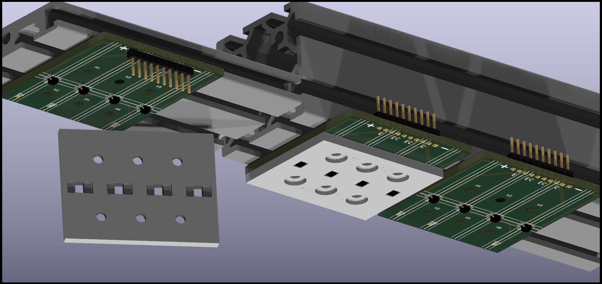
I see, to pique the interest of the clique so people make an appropriate piano clack, you guys need a few thousands of words, aka pictures. Here you are!
things explained here for the previous one and
things explained here for the last picture (link different from the other one!)
@JayKominek if you can find the time to give even a cursory look at these boards (you might want to use the PRs) I'd greatly appreciate that. I suspect I may have made some glaring mistake and I'd love to learn before making an order, which I hope to make this week. I think I am done fiddling with them. Thanks!!
If any of you want to have some stubs in your hands, print the following pages (make sure you are really printing at 100% for example checking that your 4x boards are 49mm x 47mm) and then cut them with scissors.
(if there's interest I can push these to github which seemed unnecessary clutter)
EDIT: These two files got inadvertently deleted as described at https://pianoclack.com/forum/d/1222-i-have-inadvertently-deleted-some-files-on-the-forum/17 and I am not spending the time to re-upload it unless someone asks
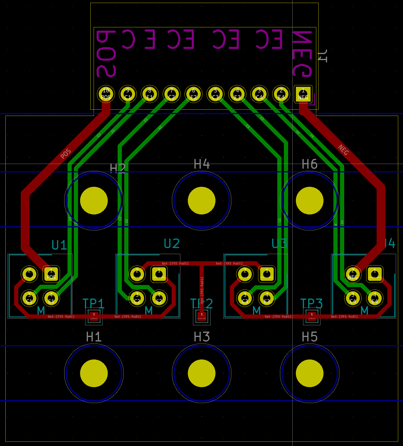
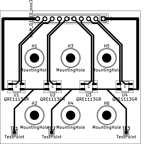
Since there was some, uh, general interest in PCB layout above, I'll comment here. I'm using the 4x sensor board as an example, but the same issues were present on the 2x board.
I didn't check pinouts very hard, but assuming they're right, the board should work fine.
Reiterating: board should work fine.
Layout could be better, for free, though. Nit-picking commences:
Apropos of the autorouter discussion, for it to be good at laying out something as simple as this board, you'd need it to know:
(I'm not aware of ever having worked on, or seen, a board which was laid out with an autorouter.)
(But Jay, some of your early boards didn't do things you said to do above! Yeah, I've gotten a lot of layout practice on this project, and spent a bunch of time reading Electromagnetic Compatibility Engineering.)
Awesome thanks a lot for this feedbac! Obviously I knew close to nothing about the best ways to make the board easier to solder. Some comments and one follow up question
There aren't any surface mount pads that count on this one, I kept the signal traces (which all happen to be green) extremely close on this one, without adding any unnecessary bends. (They could be slightly closer for U2 and U3, both at the top and the bottom, but, ehhh.) I do add some space between power and signal, beyond the fact that they're on separate layers, but I do it by adding the wiggling to the power traces. I do enter some of those square through hole pads diagonally, but they're already getting waaaay more heat and solder than an SMT pad ever would.
Here is an update.
If everything looks good (besides 2 which I am working on now) I'll update the PR accordingly (and for the 2x board too)
Thanks a lot once again!
Updated PR of 4x as discussed, here is my current proposal. Add some bends to the tracks, but I think the benefits of keeping them close outweights the cost.
As a beginner in PCB manufacturing, I liked the easyeda.com editor. There is also automatic tracing and you can immediately order the manufacture of boards on jlcpcb.
scherbakov.al As a beginner in PCB manufacturing, I liked the easyeda.com editor. There is also automatic tracing and you can immediately order the manufacture of boards on jlcpcb.
Does the automatic order submission and tracking include assembly or is it only for PCB manufacturing?
I've found that ordering PCB alone is tedious but doable, but I am yet to figure out what the various places want for ordering assembly…. which I definitely want because as Jay said "I'm sure as hell not tweaking 384 knobs" I say that I'm sure as hell not soldering 176 sensors, or even 176/4 boards since for SMT one can simply bake the board and solder 4 sensors at the time 😉
In any case, I am not making my own boards from zero here, but following the footprints of the giants, hoping to stand on their shoulders one day, so going "my way" (e.g. with EasyEDA) means that I won't be able to do that….
RIP Does the automatic order submission and tracking include assembly or is it only for PCB manufacturing?
Yes, you can order boards with components installed on them. Their minimum order is 5 boards, 2 of which can be assembled with component placement. It is not expensive to place small surface details on the board. The installation of through components is expensive. I ordered boards and assemblies for several ICs and 2040 size resistors. Soldering such small parts in large quantities would have been extremely tedious and impossible in my current environment. But I soldered the optical sensors myself. I was very pleased with this service.
scherbakov.al Yes, you can order boards with components installed on them.
Thanks! Maybe I'll give that a try, then. In fact, submitting JLCPCB requested assembly data via the regular webform is an exercise in frustration. We'll see if EasyEDA can cleanly import KiCad files.
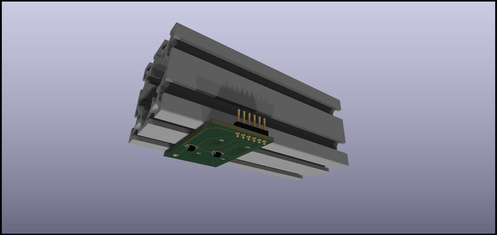
I've been silently working on and off on this, and I now have a question. For the hammer sensors, I am almost settled to the design mentioned above, which looks like this:
This works mechanically good, based on my cardboard models. In case it's not clear, you are looking at the sensors (those four black things on the green PCB) from the bottom. The hammers will hit them.
Now, for the damper sensors, the best approach would be to use a similar (note 1) board. The best way to mount that would be to use an extrusion like https://us.misumi-ec.com/vona2/detail/110302261730/?ProductCode=HFSQN4-1030-1382 to mount them under the keys, on the back where the back action is (or would be if it's removed). The problem is that header to attach the jumper connectors. It can't be in that direction, since that goes below the Keybed. One option could be to use angled connectors, but that has other complications that I don't want to get into, so my preference would be to simply mount the connector on the other side of the board, namely the same as where the sensors are.
The problem with that is that the soldering would be on the wrong side of the PCB, so the question for people who know more about that than I is if I could use the same mounting hole as a via, or if I need a separate via for that. As always, other solutions/ideas are well accepted and sought after.
(note1): since there is an extremely high cost for setup, having 176/4 + spare boards that are all identical would be most ideal, rather than 88/4 boards of one kind and 88/4 boards of another, which would cost more than double than having everything identical (I have already studied how to make sure that I can use boards with 4 sensors even though none of my hammer sections is made of a multiple of four hammers -- obviously there will be unused/unconnected sensors, the problem was that the spare one might be in the way).
I am not sure if the volume price would apply for an assembly of the jumper of two sides, but I hope so.
RIP The hammers will hit them
My intuition tells me hammering the electronics directly is wrong. I can't explain why, maybe I'm wrong but I don't find that right, it will certainly stop working after a while. Of course, you can experiment and prove me wrong 😀
CyberGene My intuition tells me hammering the electronics directly is wrong.
You arrive late to this party: it has already been discussed at nauseam 😃 and that's what @JayKominek and I have settled in. I had the same gut feeling as you do, but then settled for being good enough.
Now, back to my question…. https://electronics.stackexchange.com/questions/85292/what-pad-hole-drill-size-is-appropriate-for-a-given-through-hole-lead-diameter
RIP The problem with that is that the soldering would be on the wrong side of the PCB, so the question for people who know more about that than I is if I could use the same mounting hole as a via, or if I need a separate via for that. As always, other solutions/ideas are well accepted and sought after.
"Mounting holes" aren't electrical, especially in Kicad. But the through holes used for through hole parts like pin headers are plated, just like vias. Things like pin headers can be soldered onto either side of the board, no problem. I do that on mine.
CyberGene My intuition tells me hammering the electronics directly is wrong. I can't explain why, maybe I'm wrong but I don't find that right, it will certainly stop working after a while.
The sensors themselves are potted in epoxy. Their failure is wildly unlikely. I'd expect the solder joints between them and the PCB to fail first. PCBs themselves have enough flex that I'd expect the traces to survive indefinitely.
Personally I've got little 3D printed protector things, so that the hammers strike those (and are kept 2mm away from the sensor surface), and the force is distributed across the whole PCB. I then put some very thick electrical tape on the back side to cushion the interface between the PCB and the rail.
RIP Now, back to my question….
If you're going for automated / professional assembly, that's probably a question for the assembler.
If you're doing it by hand, then a very gentle press fit is probably ideal.
Solder will bridge the gap of any sane drill size, but it'll take a lot more solder (mostly a problem for hand assembly), and you increase the risk of parts falling out,
JayKominek "Mounting holes" aren't electrical, especially in Kicad. But the through holes used for through hole parts like pin headers are plated, just like vias. Things like pin headers can be soldered onto either side of the board, no problem.
Awesome.
JayKominek If you're going for automated / professional assembly, that's probably a question for the assembler.
Sounds great, I'll ask then.
JayKominek If you're doing it by hand, then a very gentle press fit is probably ideal.
Thanks a lot for the tips!
CyberGene My intuition tells me hammering the electronics directly is wrong.
In my old Clav each key lever "hammers" upon its rubber contact.
And the rubber "hammers" upon the underlying PCB contacts.
Yes, they wear out eventually. But doesn't everything?
Digital piano actions are to a certain degree inconsistent in velocity detection because they rely on mechanical switches that will deteriorate from the constant banging. Optical contactless sensors can eliminate the wear. But if they are robust enough, they can take some beating.
I’d be also worried about vibrations in the rail causing neighboring sensors to oscillate longitudinally which can potentially reduce the precision of proximity detection but I guess that can be solved through using a very rigid rail that is fixed at multiple points.
CyberGene I’d be also worried about vibrations in the rail causing neighboring sensors to oscillate longitudinally which can potentially reduce the precision of proximity detection but I guess that can be solved through using a very rigid rail that is fixed at multiple points.
I was worried about that too. The flex computation from the specs did not help my "gut feeling". Holding that aluminum extrusion which you can see on the rendering I posted earlier today, did. That extrusion is really, really rigid. If you think the flex computation can help, the specs are on the misumi website.
CyberGene But if they are robust enough, they can take some beating.
JayKominek Personally I've got little 3D printed protector things, so that the hammers strike those
I could do the same thing Jay did, which you can see at https://github.com/jkominek/piano-conversion/tree/master/mechanical (I thought I saw a picture once, but can't find it right now). With the smaller sensors will actually be much easier to align and more effective since the "hole" would be much smaller and protective. I have just too many balls to juggle at the moment, but if anybody is interested in this design, and could do the 3D model for that, it'd be a nice plus. But it's just a plus, I'm confident it'll get years of service even without. The perfect is the enemy of the good, and if I try to do everything perfectly, I'll end up never finishing (which some days already feels like it)