JayKominek
- Generally not a bad plan to keep the signals away from the power, but these power traces shouldn't be generating (much? any?) noise, compared to what you'd see attaching a switch mode power supply to a microcontroller, or similar. It's a linear supply feeding LEDs. The only variation will be from the LEDs aging, or the temperature in the room changing.
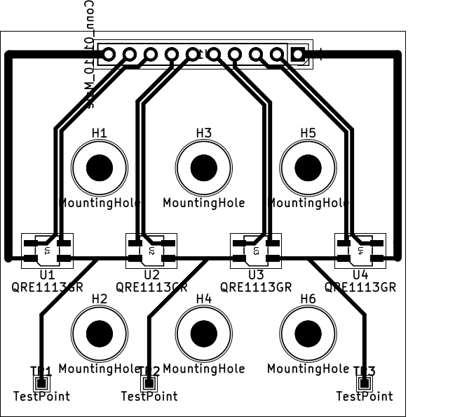
- The trace pairs should be as close as manufacturing tolerances allow. I think I failed to do that on one of my early layouts. I've attached a screenshot of what the current layout looks.
- 👍
- I'd at least consider doing exactly that. (Or just don't worry about making them thicker. It just means you'll dissipate some of the waste voltage in those traces instead of in the MOSFET on the LED power board.) With solid ground pours, you've got to do it (it is called "thermal relief", if you look in the configuration options for a ground plane in Kicad), with thick traces, there's no automatic mechanism. If you look on my ADC or LED board layouts, I think I've got some spots where I bring thick power traces to a regulator, or diode or something, and narrow it down right at the last moment. Generally because I had difficulty hand soldering that exact spot in one of my early revs.
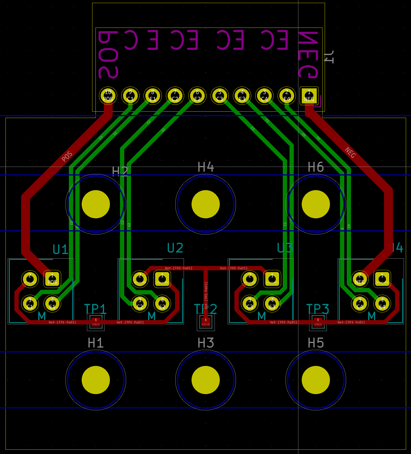
There aren't any surface mount pads that count on this one, I kept the signal traces (which all happen to be green) extremely close on this one, without adding any unnecessary bends. (They could be slightly closer for U2 and U3, both at the top and the bottom, but, ehhh.) I do add some space between power and signal, beyond the fact that they're on separate layers, but I do it by adding the wiggling to the power traces. I do enter some of those square through hole pads diagonally, but they're already getting waaaay more heat and solder than an SMT pad ever would.