Skip to content

Update on piano conversion

RIP

JayKominek The default minimum track spacing is conservative and pretty safe for this project.

I was actually thinking of my modifications, for example this one:
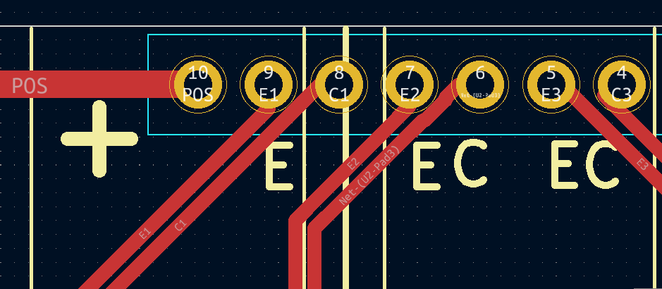
And I guess the majority of my insecurity comes from not fully knowing notation and the process here. What are those thin rings around the thick rings? Should have been both tracks for pad 5 and 4 more to the right to a) stay closer and b) avoid that notch on the pad 4 connection?
Another thing that confused me is the warnings of silkscreen being "erased" by the copper tracks. Aren't the copper tracks covered by an insulating material on top of which stuff can be written? And uncovered only in the areas where soldering is expected? It seems so in the raytracing 3D view, but the warning seems to indicate otherwise.

Also, when ordering or requesting for an estimate, I need to select the accuracy I want (sigh, can't they figure it out from the file I'm uploading???) and I could use 8mil which is slightly more than the 0.2mm selected in KiCad, so I selected 6mil, which costs (marginally) more but more importantly prevents the use of the 2oz Cu density (which may be overkill, but it's almost free at 8mil accuracy)…. Probably none of these matters but still it takes a toll on my decision making….
Drew-r

@RIP, is that a diy avatar or stock? Either way, a very good likeness! 😀


JayKominek

RIP What are those thin rings around the thick rings?

The clearance that needs to be maintained by unrelated nets. You might note that the track for Net-(U2-Pad3) makes a tiny little jog around pad 7's ring.

RIP Should have been both tracks for pad 5 and 4 more to the right

The track to pad 5 (net E3), looks fine in that picture. The track to pad 4 has some wasted copper, where it looks like the track tried to go to the left and then you brought it back, but it won't have any negative consequences.

RIP Another thing that confused me is the warnings of silkscreen being "erased" by the copper tracks.

Are you sure it is referring to tracks, or to the copper of the pads? You've got silkscreen going over pads 8 and 7 in that picture, which, as it warns, will have to be omitted.

You're right that copper which isn't intended to be soldered to will be covered by solder mask, and is a legitimate place to put silkscreen. That just doesn't apply to all of your copper.

RIP I need to select the accuracy I want (sigh, can't they figure it out from the file I'm uploading???)

Perhaps you want even tighter tolerances than what appears in the file. How would they figure that out?

If you specified 8, they might catch it and warn you when they do a manual review. Not all of these checks boardhouses have are fit for generating automatic feedback to customers.

RIP I selected 6mil, which costs (marginally) more but more importantly prevents the use of the 2oz Cu density (which may be overkill, but it's almost free at 8mil accuracy)….

Absolutely no need for 2oz copper on the sensorboards. The only value is for carrying higher currents.

I'd pay for the service which matches the tolerances you used, the risk/reward/frustration tradeoff isn't great for trying to save those pennies.


RIP

JayKominek The clearance that needs to be maintained by unrelated nets. You might note that the track for Net-(U2-Pad3) makes a tiny little jog around pad 7's ring.

Ah! I thought that was my unstable hand when making the track! Should I further need to tweak the board will take that out.

JayKominek The track to pad 5 (net E3), looks fine in that picture. The track to pad 4 has some wasted copper, where it looks like the track tried to go to the left and then you brought it back, but it won't have any negative consequences.

Thanks so much, I appreciate the clarification. Should I further need to tweak the board will take that out.

JayKominek Del Vento Another thing that confused me is the warnings of silkscreen being "erased" by the copper tracks.

Are you sure it is referring to tracks, or to the copper of the pads? You've got silkscreen going over pads 8 and 7 in that picture, which, as it warns, will have to be omitted.

You're right that copper which isn't intended to be soldered to will be covered by solder mask, and is a legitimate place to put silkscreen. That just doesn't apply to all of your copper.

You are right I was being sloppy with terms. What it was saying is "Silkscreen clipped by soldermask". Now, most of that I understood (places where there is actual soldermask, such as the sensor pads). Some others were weirdly termed, but still understandable (got out of the board by a fraction of a mm, so it should have said "clipped by edge cut"). Others, were probably not real warning, but just display things, such as the "plus" sign (to indicate polarity for the power supply) "disappearing" under the track when I placed it to the left of the jumper where it seemed to belong better. But on close inspection, there was no arrow pointing to that as a problem, so that was probably just a display thing of PCBEditor and would instead appeared correctly in the final board? In fact it does so on the 3D viewer…

JayKominek I'd pay for the service which matches the tolerances you used, the risk/reward/frustration tradeoff isn't great for trying to save those pennies.

In fact that's what I requested in the estimate. The only concern was of the limitation it introduced to the 2oz thickness, but…

JayKominek Absolutely no need for 2oz copper on the sensorboards.

If that is the case, then it sounds everything is fine and if I am satisfied (and they are too), I can proceed with the order.

JayKominek The only value is for carrying higher currents.

Yes, the value for higher currents I (obviously (?? 🤣 ) knew. Since it was cheaper for the less accurate process, I threw it in anyway in an earlier estimate whose order I did not complete.

I'll keep y'all posted! Hopefully this is the last or very close to last iteration!


RIP

I ordered the sensorboards (PCBs, parts and assembly/soldering of both SMT and TH) as well as the 3D protectors at PCBway as described early. Should be easy to reproduce for others, but not as easy as I hoped (I had to "recreate" the order rather than saying "let others order exactly what I did" -- link on the repo). About $400 for everything, which includes:

  • manufacturing of 60 PCB boards, in 2.4mm thickness
  • purchase of 60x4 QRE1113GR sensors and of 60 connectors
  • surface soldering of the 240 sensors on the 60 boards
  • through-hole soldering of the 60 connectors, 30 on one side and 30 on the other (as shown in the picture posted earlier in this thread)
  • manufacturing of 30 3D-printed protectors
  • shipping
  • paypal fee
  • coupon discount

Excluding the latter three items, the price is $7.26 per per sensorboard, or less than 2 dollars per sensor (the sensor itself is about half a dollar). In case you are wondering why 240 sensors rather than 176, it comes to:

  1. The register division of the keyboard in sections forces me to have a few unused sensors in each section, or order a few 2-sensor and 1-sensor boards. The latter is much more expensive because they don't have volume discount

  2. Ditto for the 3 pedals, which may require one sensorboard each (I might use something else, TBD)

  3. I need/want a number of spares in case any is damaged in transit, assembly, when wired or just if there is "infant mortality", not to mention the possibility to run tests outside the piano when that is finally assembled and I won't want to touch it.

    All of these together, with price considerations, made 240 the "best" choice

It was easier to deal with this company than with the other two I tried earlier. We'll see the quality when stuff arrives: @JayKominek I plan to give you a couple of these sensorboards, and if I will be ready a couple of cables as we discussed at on github so you can test both. If you have a spare ADC board (even rev0 and even unpopulated besides the connector), that will help me planning cable routing in practice rather than on paper. I plan on waiting for a little bit before orderding the subsequent parts, after assessing how satisfied I am with these.


RIP

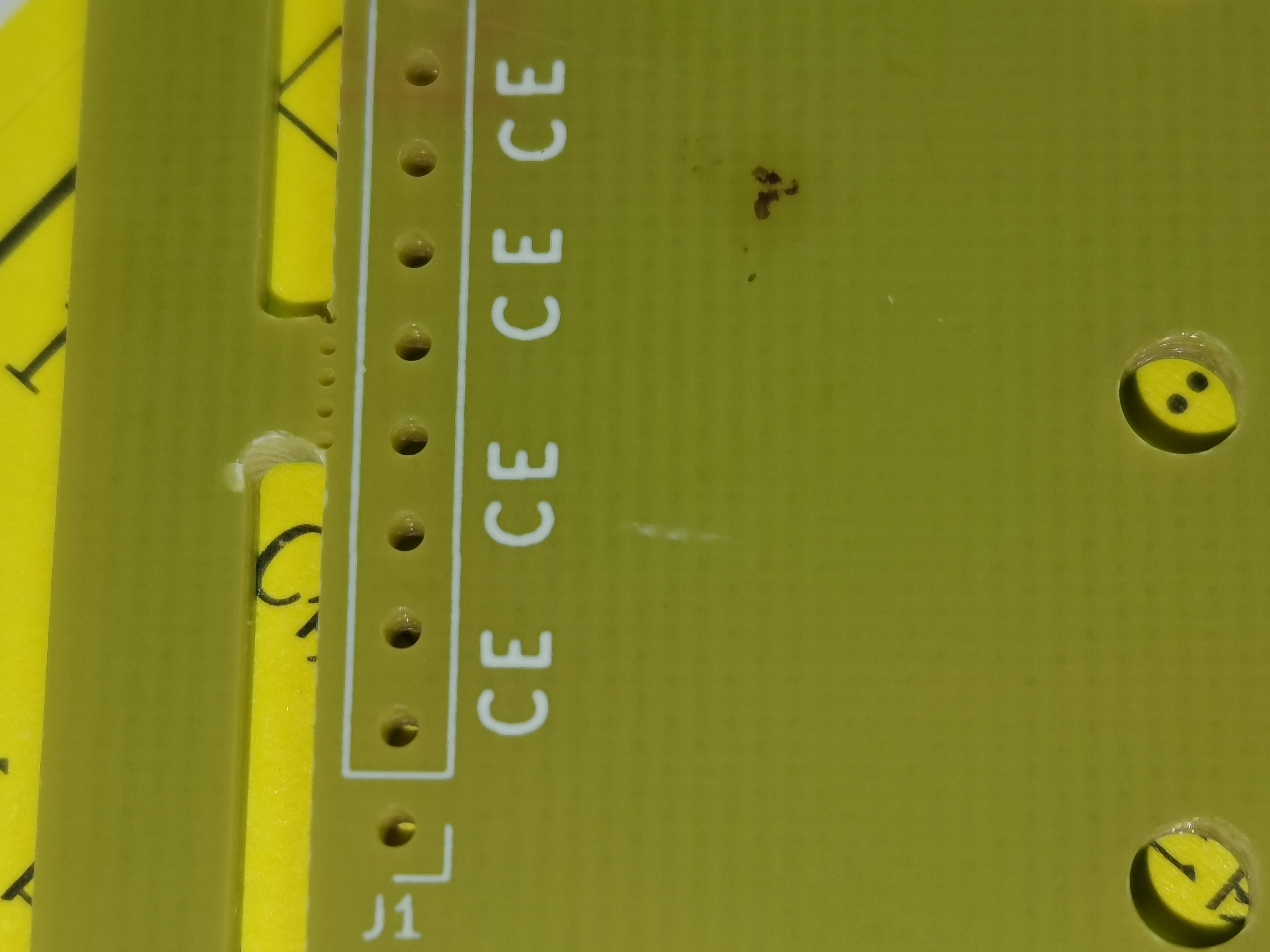
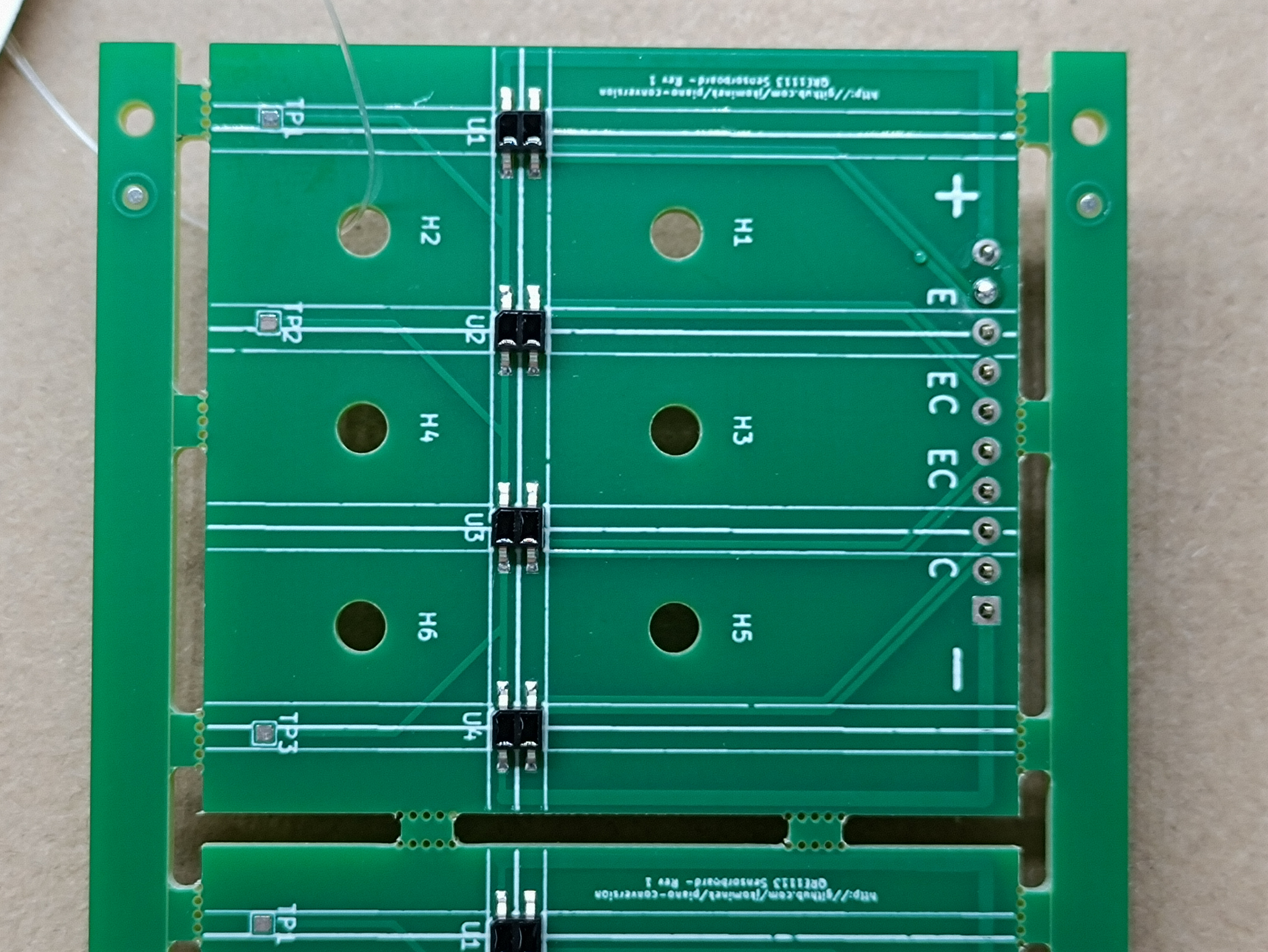
Please check the attached pictures of the assembled boards, especially the polarity or orientation of the components and tell me if there is anything wrong.

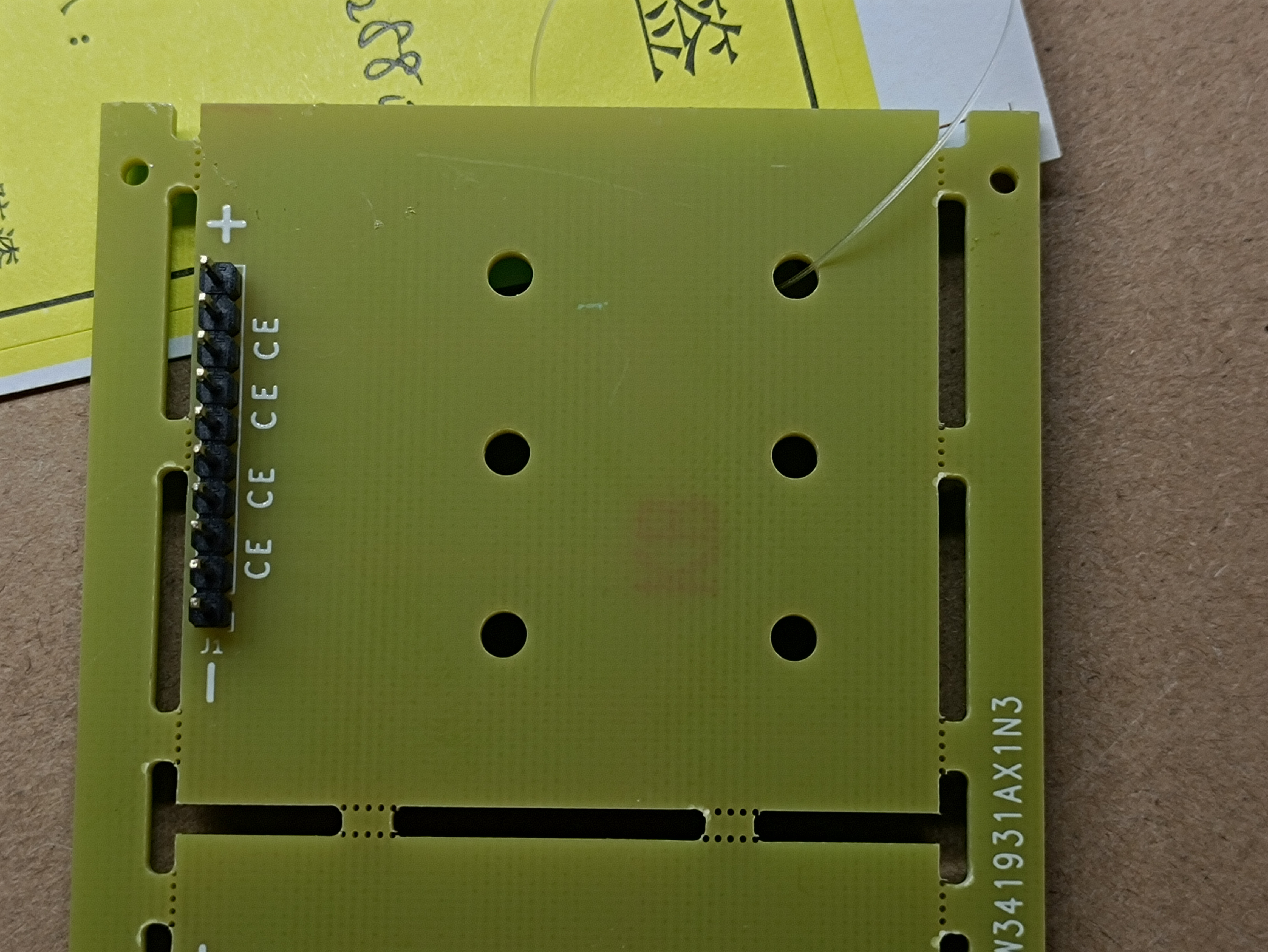
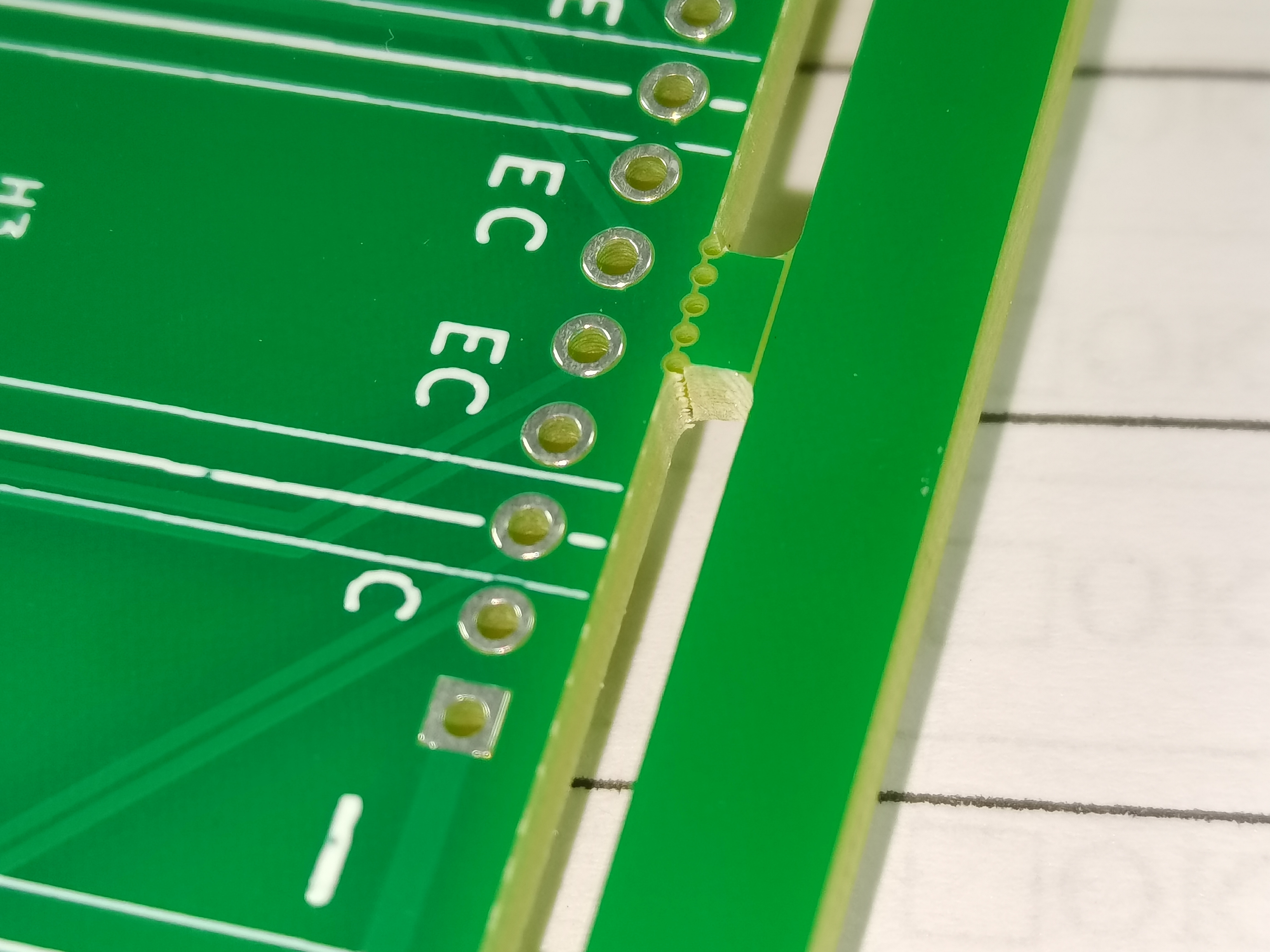
By the way, as your requirement to solder 30pcs J1 in top and 30pcs in bottom side, but this is a 1 layer board, the solder paste cannot be added in bottom side, we can only solder in top side, pls advise.

After your approval we will move to next steps.

Additional attention: Soldering for some through hole parts is not completed because we want you to confirm if there is anything wrong with the orientation. If not, solder paste will be added soon.

Alos some dirties on the board will be cleaned before shipment as well.


RIP

Obviously I replied

Thanks for your message. As far as I understand Gerber files and PCB manufacturing, the through holes for the J1 connector should be plated, just like vias. As such, soldering on the back side, even though it would not be connected "anywhere" on the back side itself, should be electrically connected on the front side. Isn't that the case with the way through holes manufactured with your process?


RIP

Their support replied

There is no copper plated inside the holes.
So I think this should be a 2 layer PCB with these holes placed both top and bottom side instead of 1 layer


RIP

The sensors PCB have arrived. I hope to post some pictures of them and of the first assembly soon 🙃😀

Meanwhile @JayKominek if you want to get a handful of the spares I have (e.g. one empty board, one populated board with one kind of connector, one with the other or whatever interests you) let me know and I'll be happy to meet you, hand them to you, and buy you coffee (or other beverage, or meal) and chat about the project if we've got time.

For the cables, there are troubles, which I will also describe here later 🤨


CyberGene

RIP, that’s a steady progress 👍🏻 What’s the remaining work?


gzpiano

Cool! It will be fun to see things working.


RIP

CyberGene Del Vento, that’s a steady progress 👍🏻 What’s the remaining work?

First would be assembling the sensorboards inside the instrument. One weekend or two will be sufficient.

Second, ADC boards. @JayKominek has the design finalized (or close, have to study them and/or ask him), but I need to do the BOM since I don't want to do 2-side surface mount assembly.

Then (in parallel) would be cables, and especially cable management. In hindsight, I should have used a different connector on the sensorboards, but now that I'm stuck with that, I need to work more on the cables.

At that point I should be able to get some close-to-final sound with some inconveniences (too many cables going to the computer and/or limited number of octaves working at the same time and/or cumbersome/unfriendly software to run on the computer)

Finally I'll need to deal with the main controller board, which again, @JayKominek has already finalized (or close) etc etc. It will remove all the inconveniences mentioned above. Its cabling should be much easier, since it's less than a dozen boards involved (unlike the sensorboards, which are many)

gzpiano Cool! It will be fun to see things working.

Tell me about that 😃 I'm really looking forward to play it!


RIP

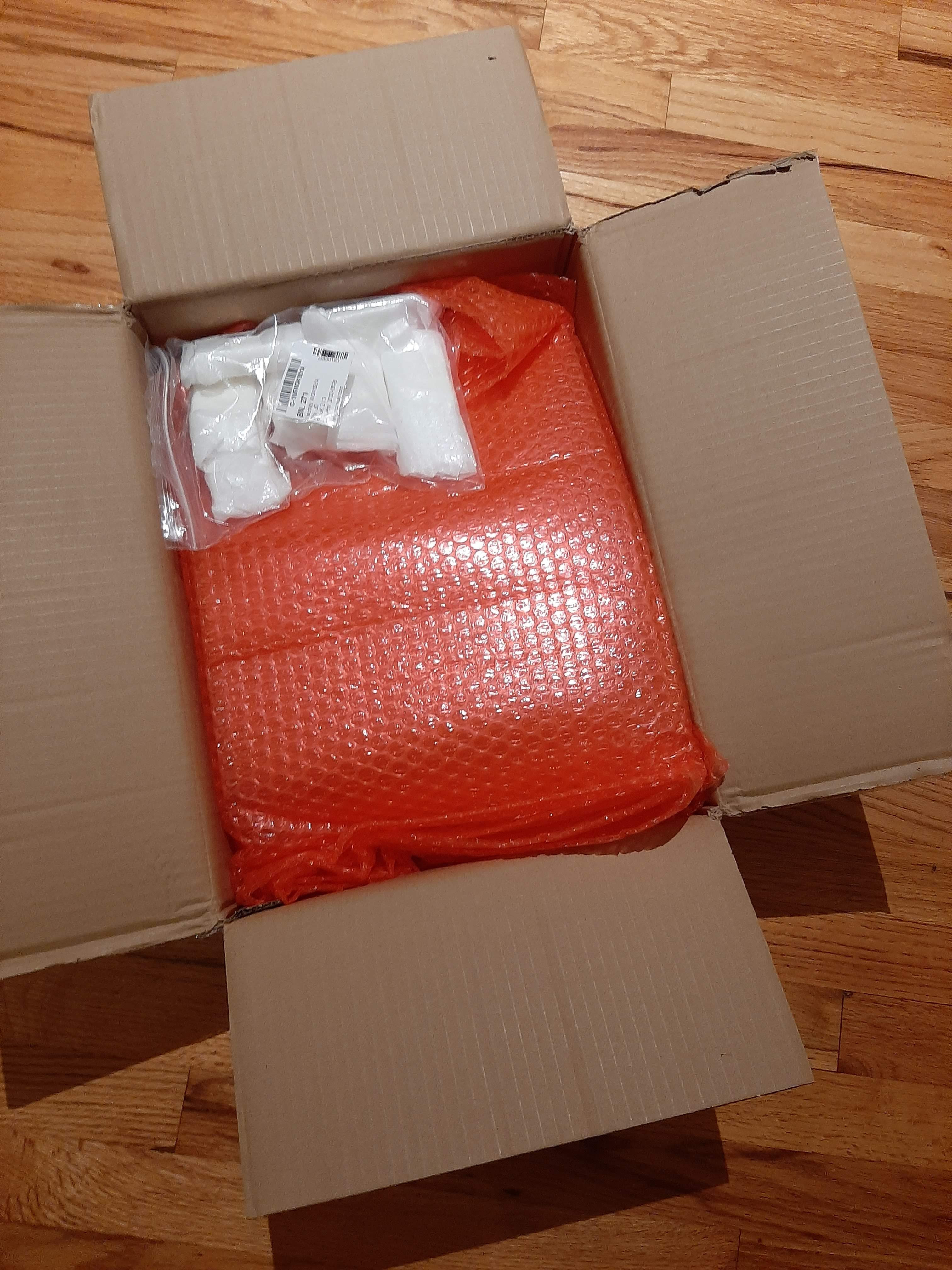
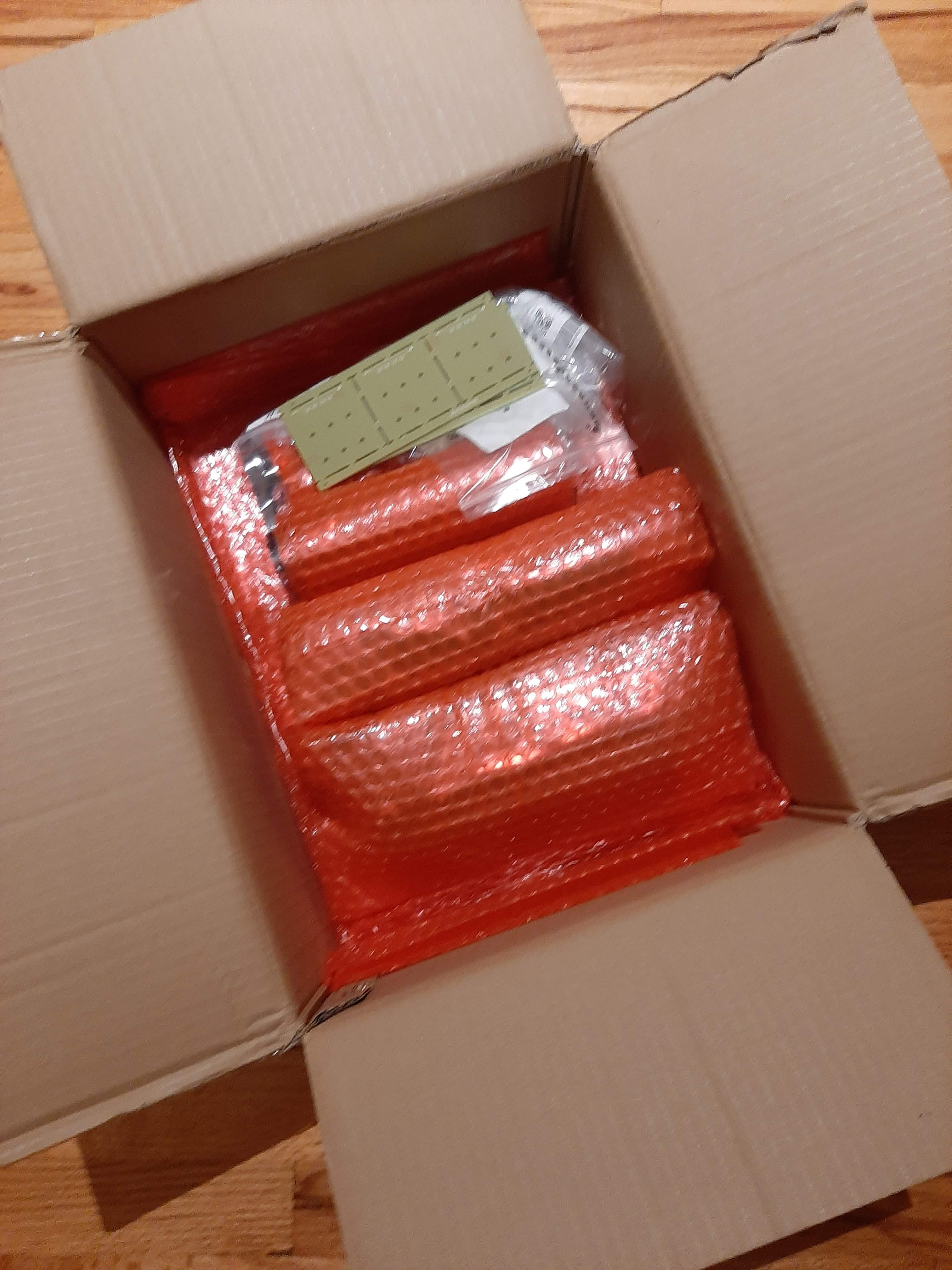
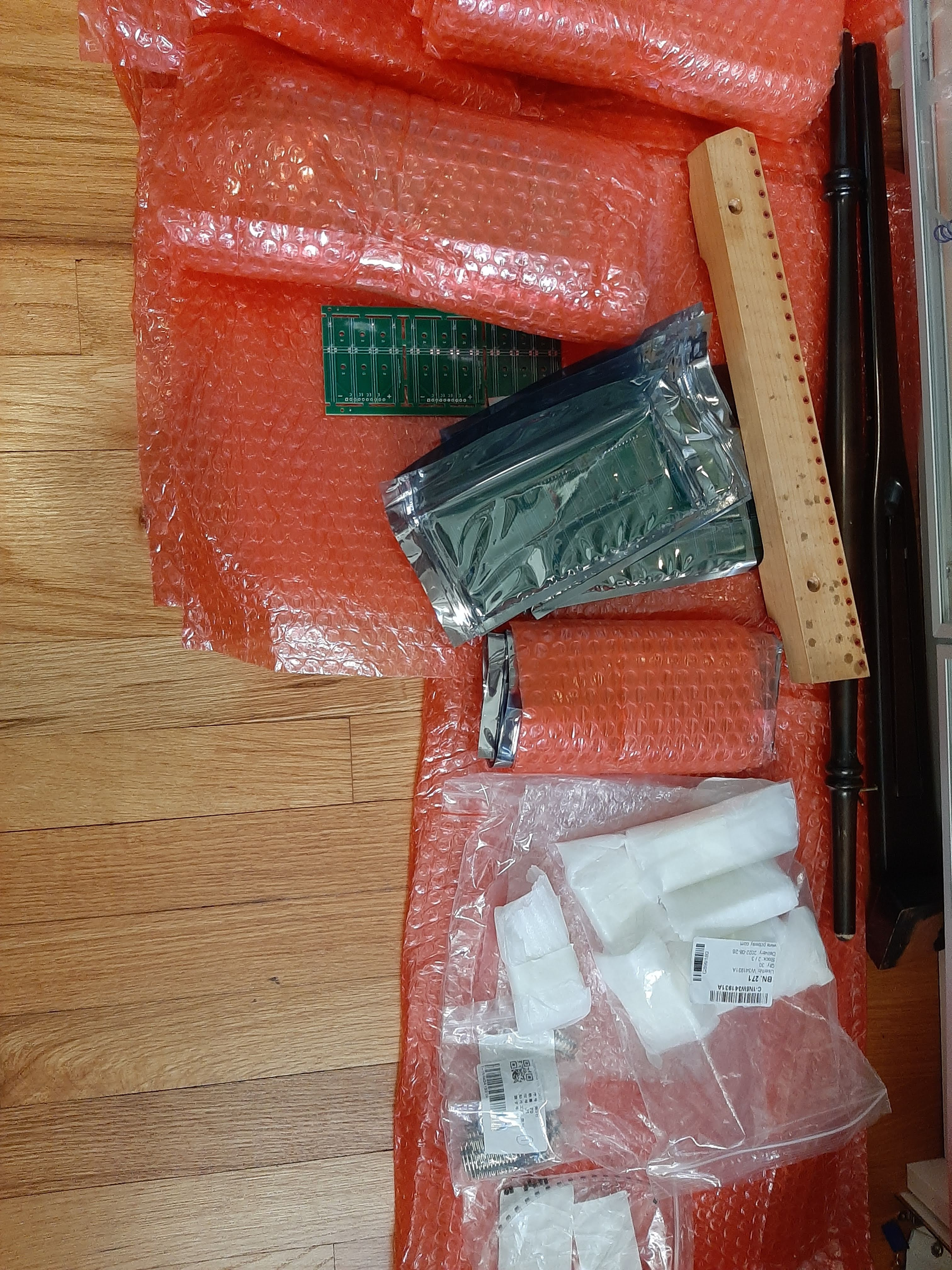
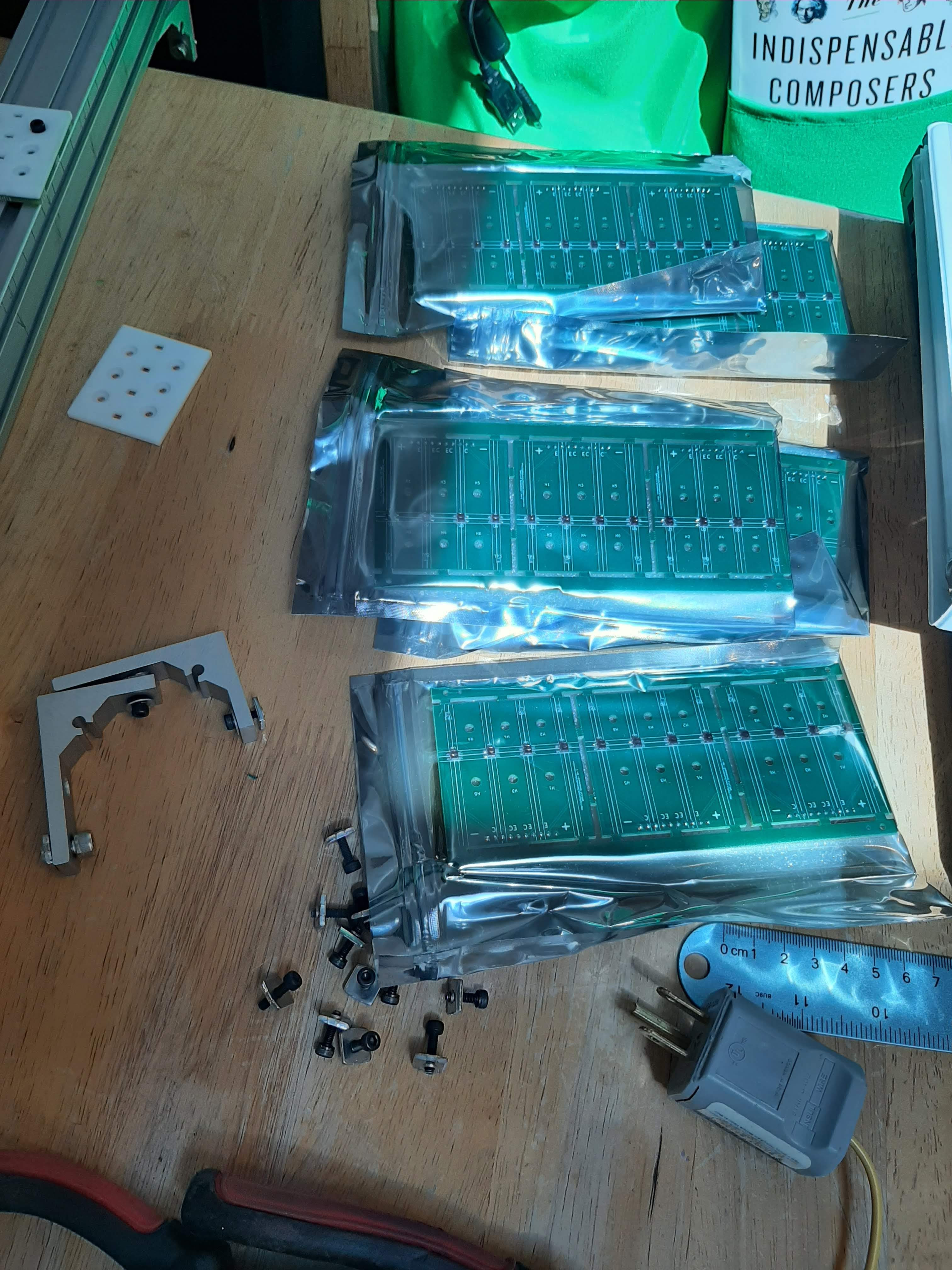
Unboxing (I could have posted this sooner, but I was eager to work on it rather than reporting…)

You may notice additional, unrelated items in the pictures, I guess that makes them unprofessional but more relatable (applies to the next posts which I will submit momentarily)


RIP

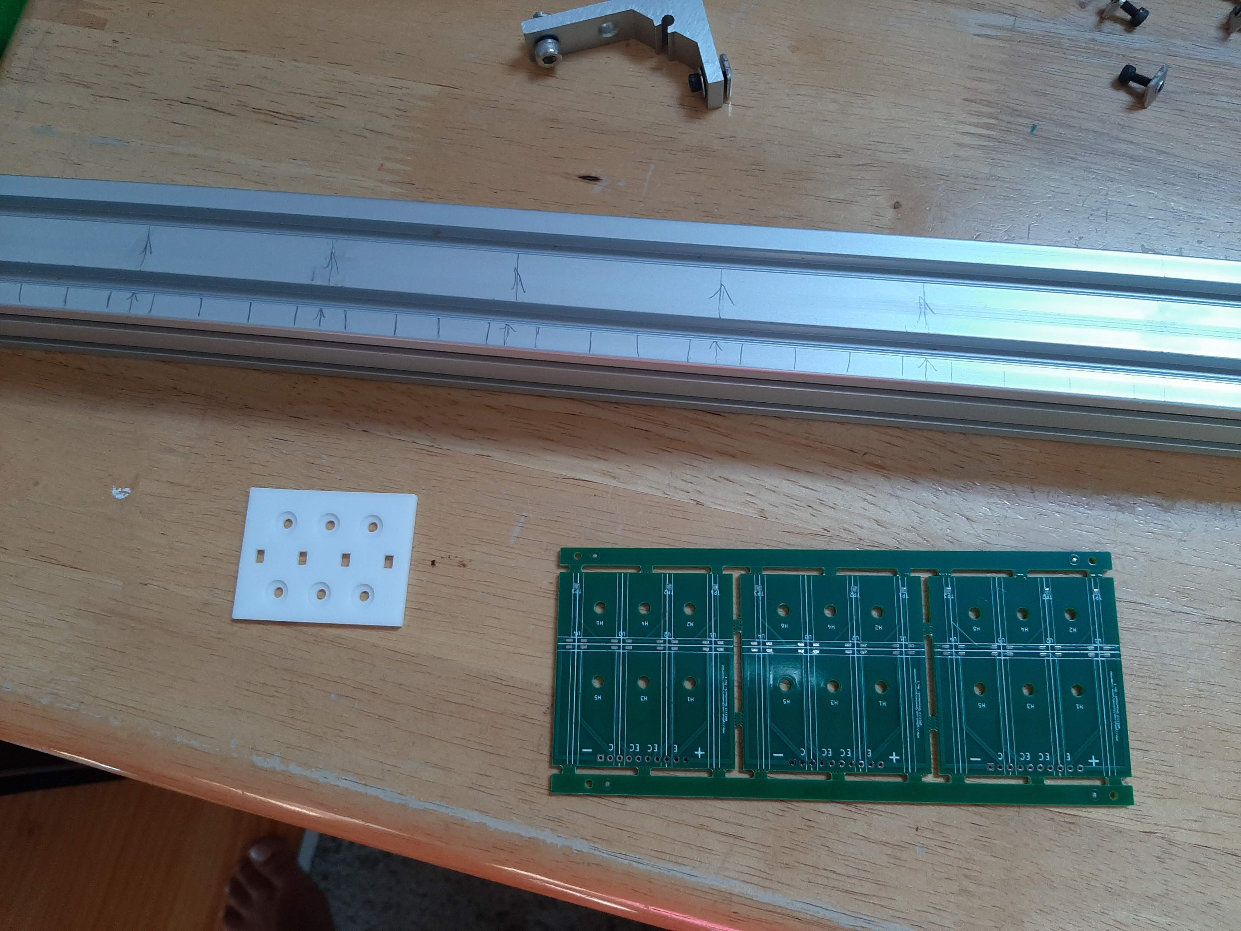
Preparing parts

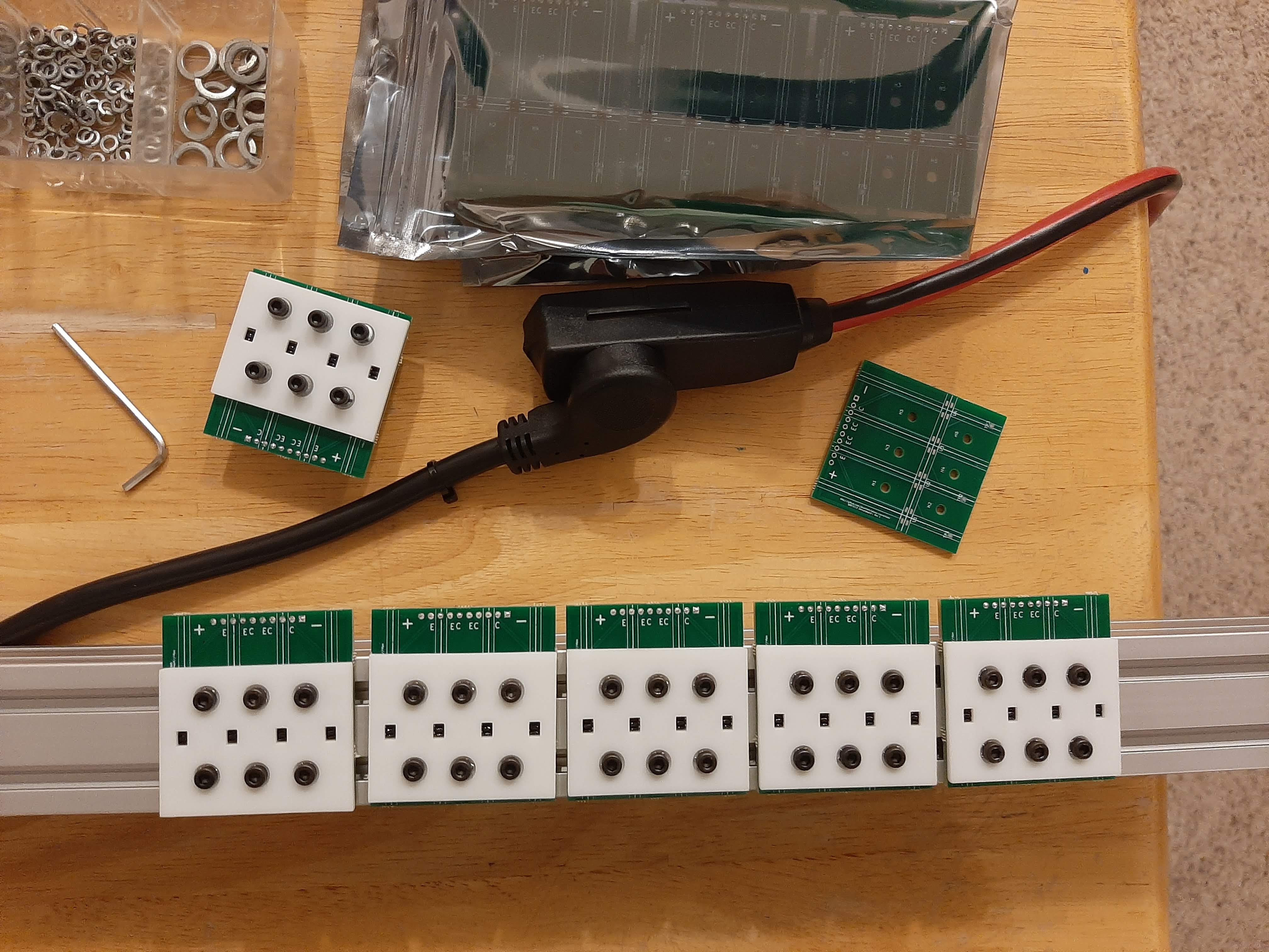
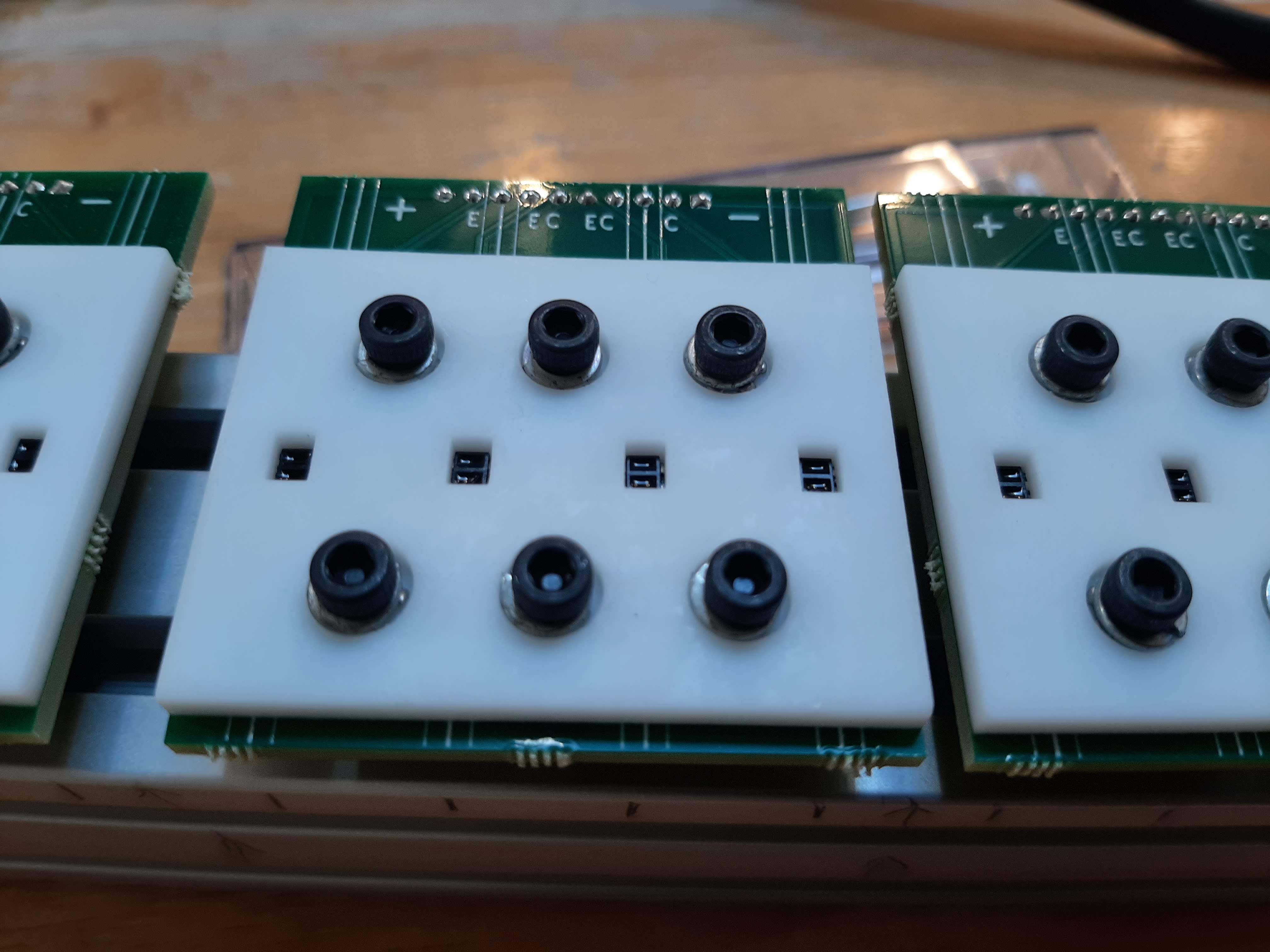
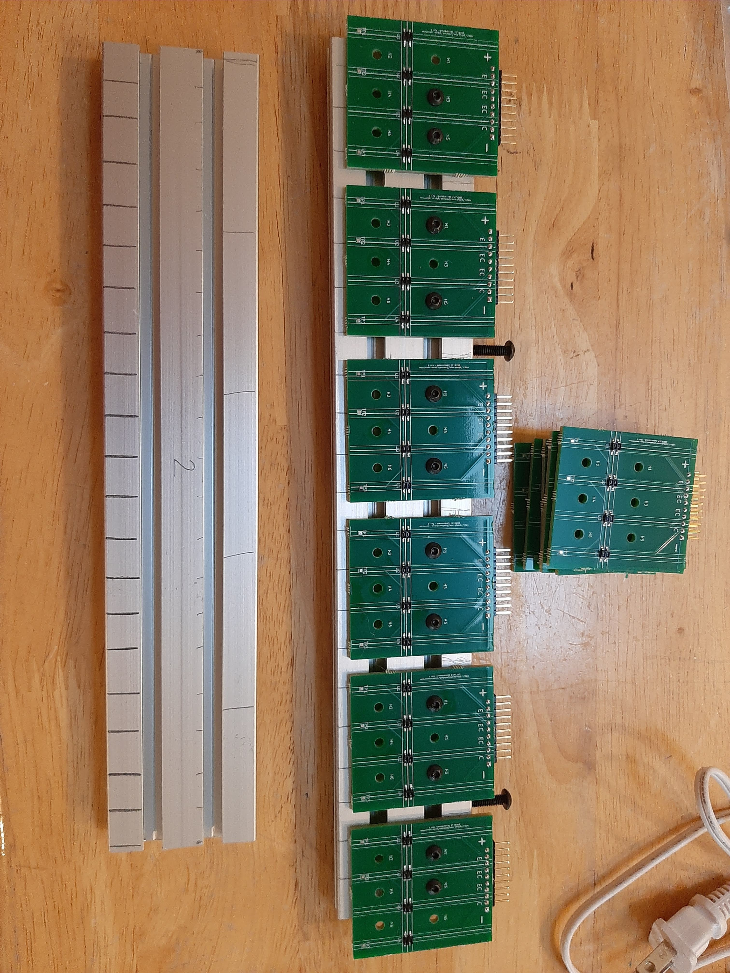
Aluminum extrusion for holding hammer sensors with marked position for the hammers and paneled (spare, unpopulated) sensorboard with its matching 3D-printed protector. Those 3D-printed items were purchased from the same company which made the PCBs and their assembly (see earlier in this conversation for details)

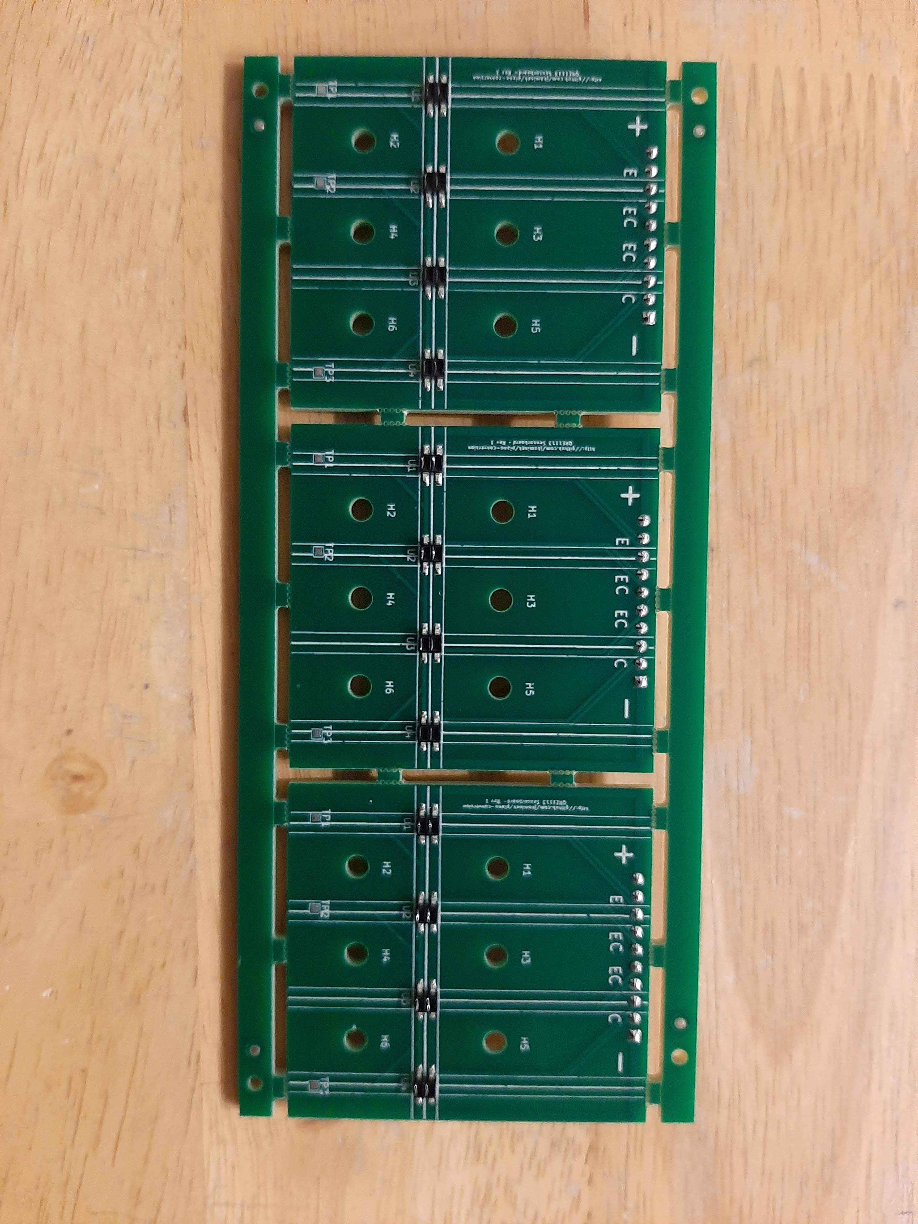
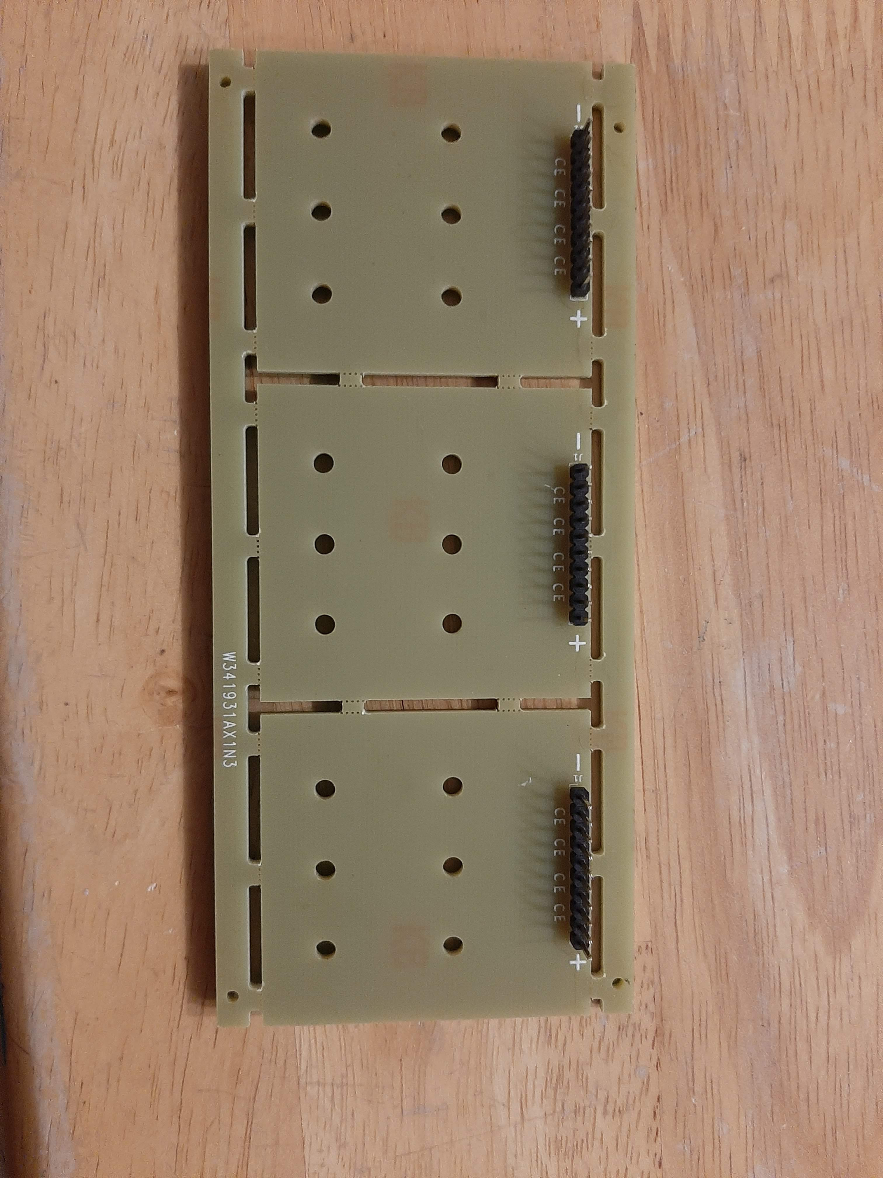
Actual, professionally assembled, paneled, populated sensorboard, front and back

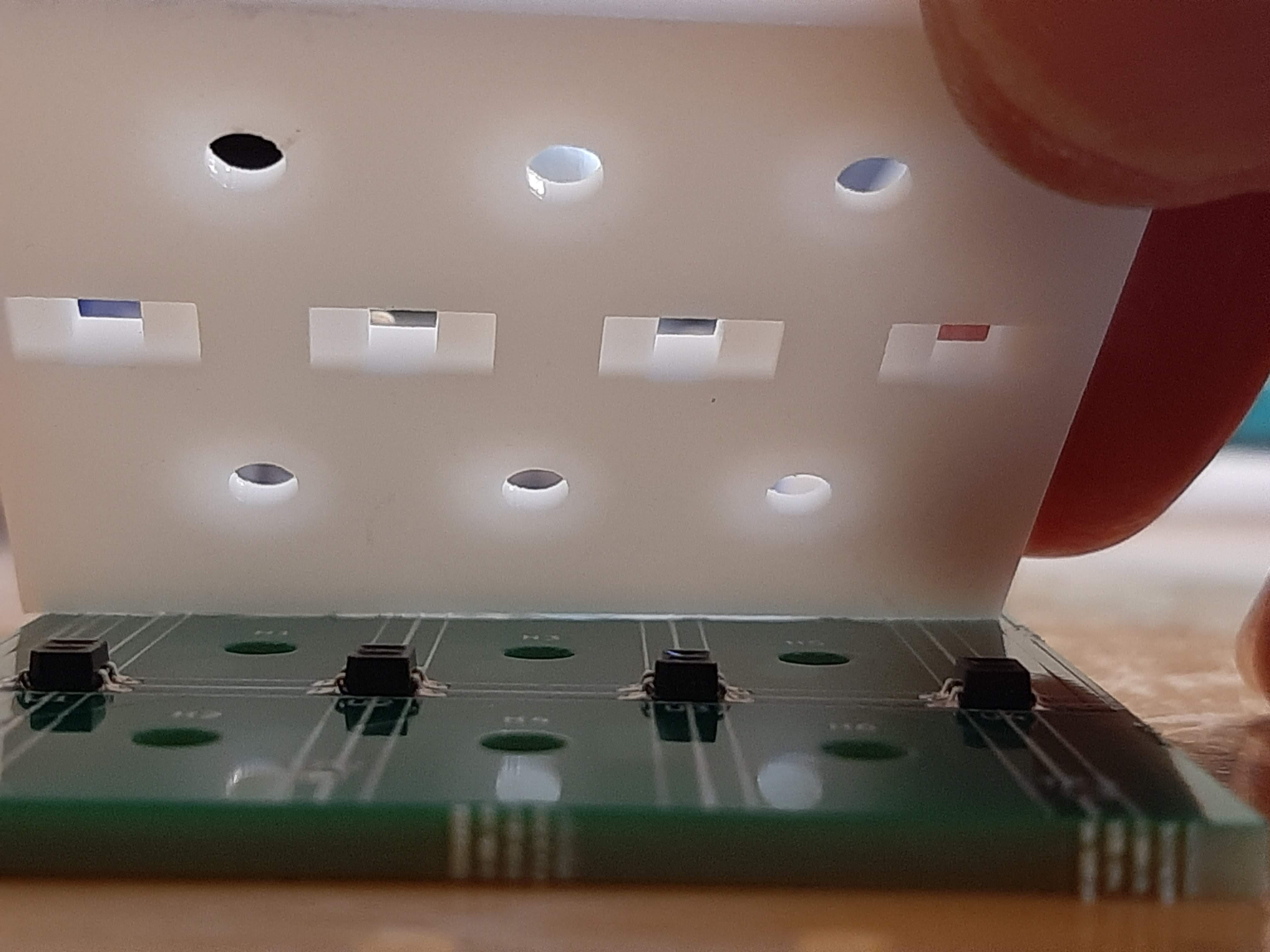
Separated sensorboard with matching protector, back and forth. Notice how the protectors allow for plenty of slack on lead connectors. Notice also the guidelines on the silkscreen, which turned out to be a very convenient thing I added to the sensorboards: they simplify alignment even when you can't see the sensor (or if you can see it at an angle and not sure of what perspective correction your brain is implementing). Only downside is that the paneling breaks are not aligned with the silkscreen guidelines too 🤣


RIP

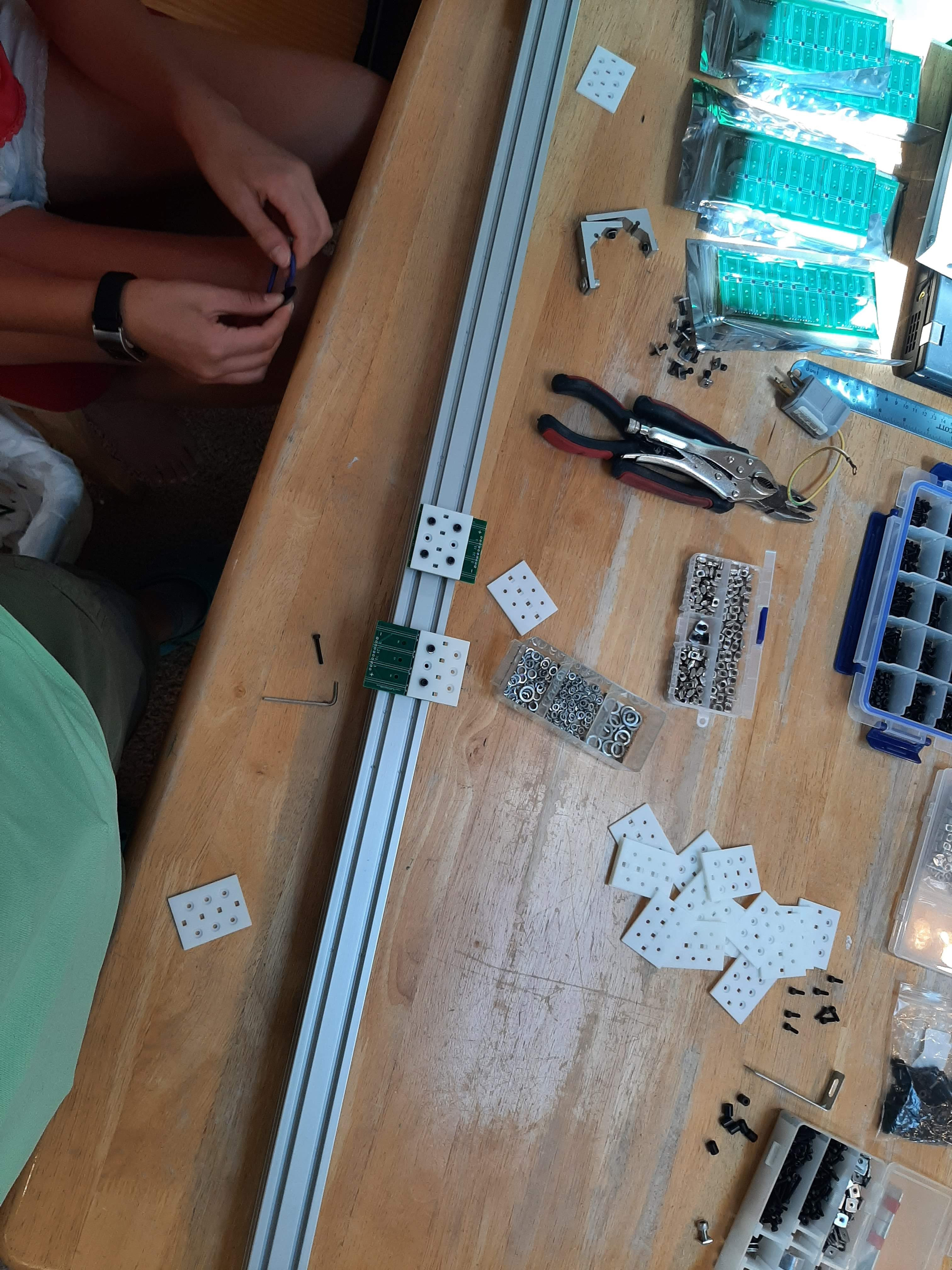
Assembling the hammer sensors on their rail extrusion. Note that this rail is a long, whole one, for both bass and treble (more on that later in this same post).

Gathering parts

First ones on the rail 😃 (not aligned yet)

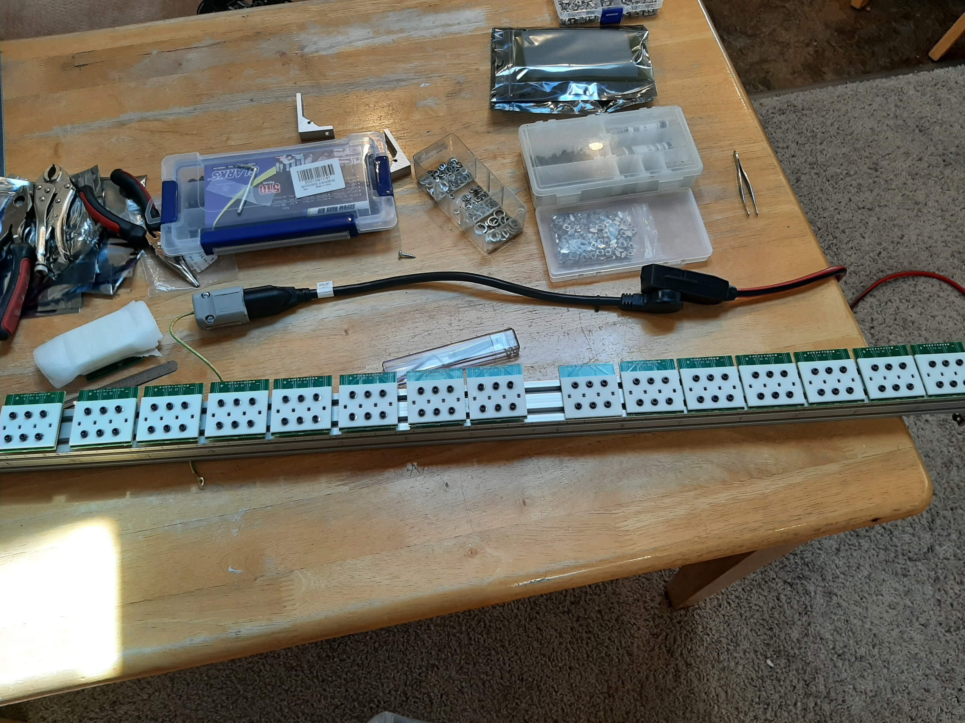
Heck, that's a lot of sensorboards!

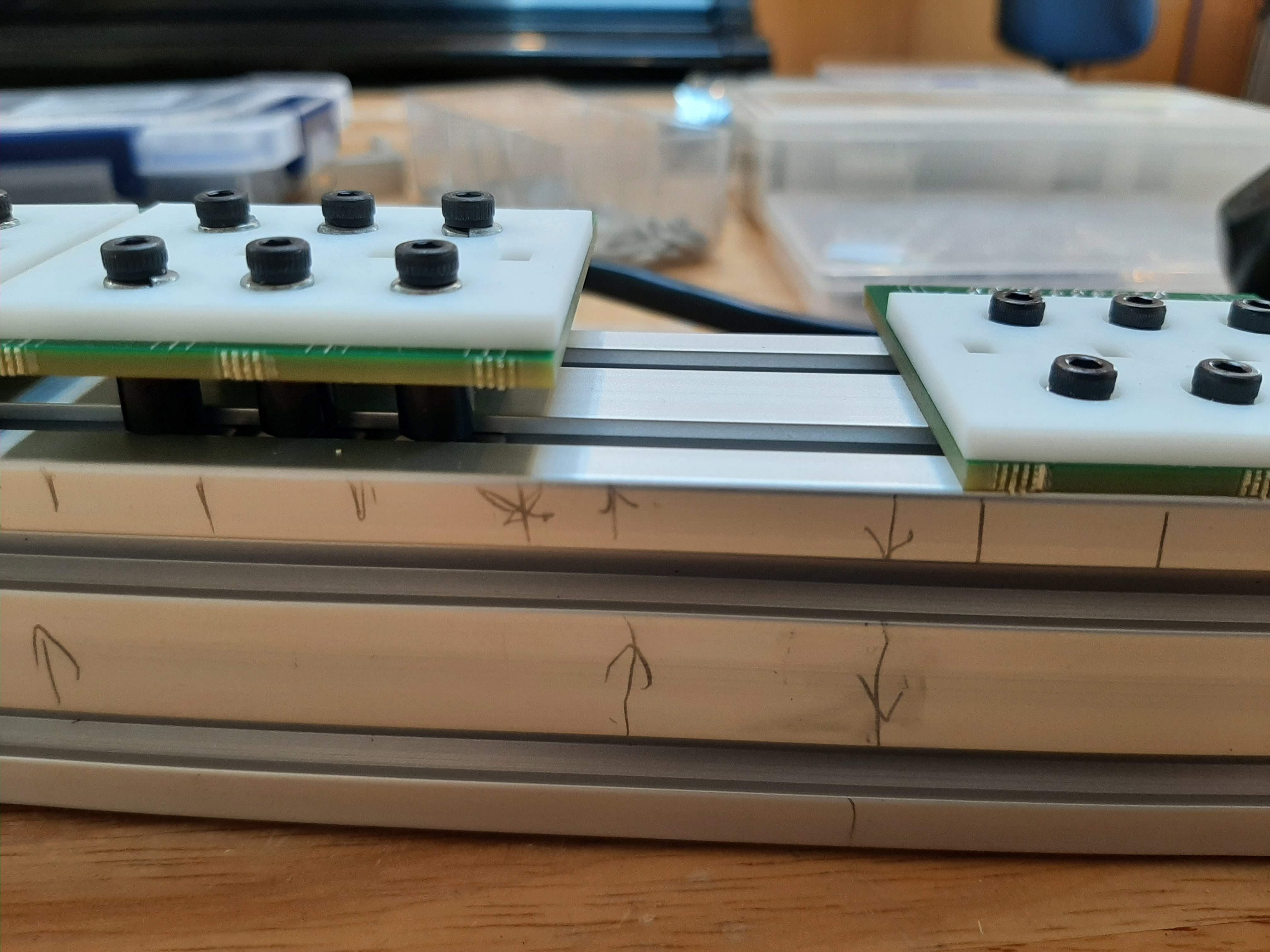
Look how nicely they fit! If there is ONE takeway that you may want to take from all this report, it is that I'm really pleased with how the QRE1113 sensors turned out mechanically: really really well for both the hammers (what you are seeing below) and the key (next post) sensorboards. These protectors are really snug, but not too tight.. not sure they'd be so if I made the 3D printing and the soldering myself. They will prevent hammers from getting too close, which will solve that "last mm" problem discussed elsewhere in these conversations. They are SMT, so there is nothing (as shown in the previous post) touching the aluminum and risking shorting, even after years of pounding. Not clear in this picture, but their small dimensions, with the guidelines on the silkscreen make it really easy to align with the hammers or keys. I am convinced that if I used the CNY70 I'd have been somewhat unsatisfied with all of these!

Notice the spacers at the bass/treble break, to accommodate for the way the action was built (which was done so because of the different string height due to the cross-stringing)


RIP

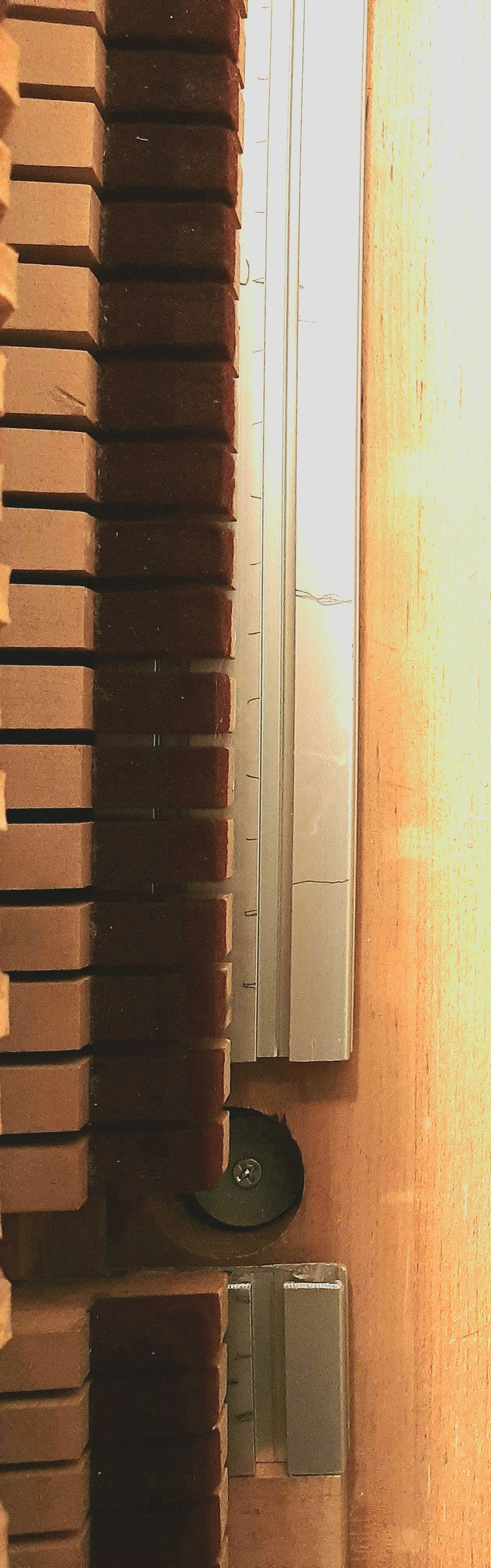
Marking the key sensor extrusion for position. Notice that because of various other components, the key sensor extrusion is sectional, rather than whole as the hammer sensor extrusion. However, sitting on the keybed, that's not a complication (as it would have been for the hammer sensor extrusion, which would have required complicated way of being held in place if it were sectional)

One section completed and the next ready. Notice the preliminary alignment of the silkscreen guidelines with the markings on the extrusion.

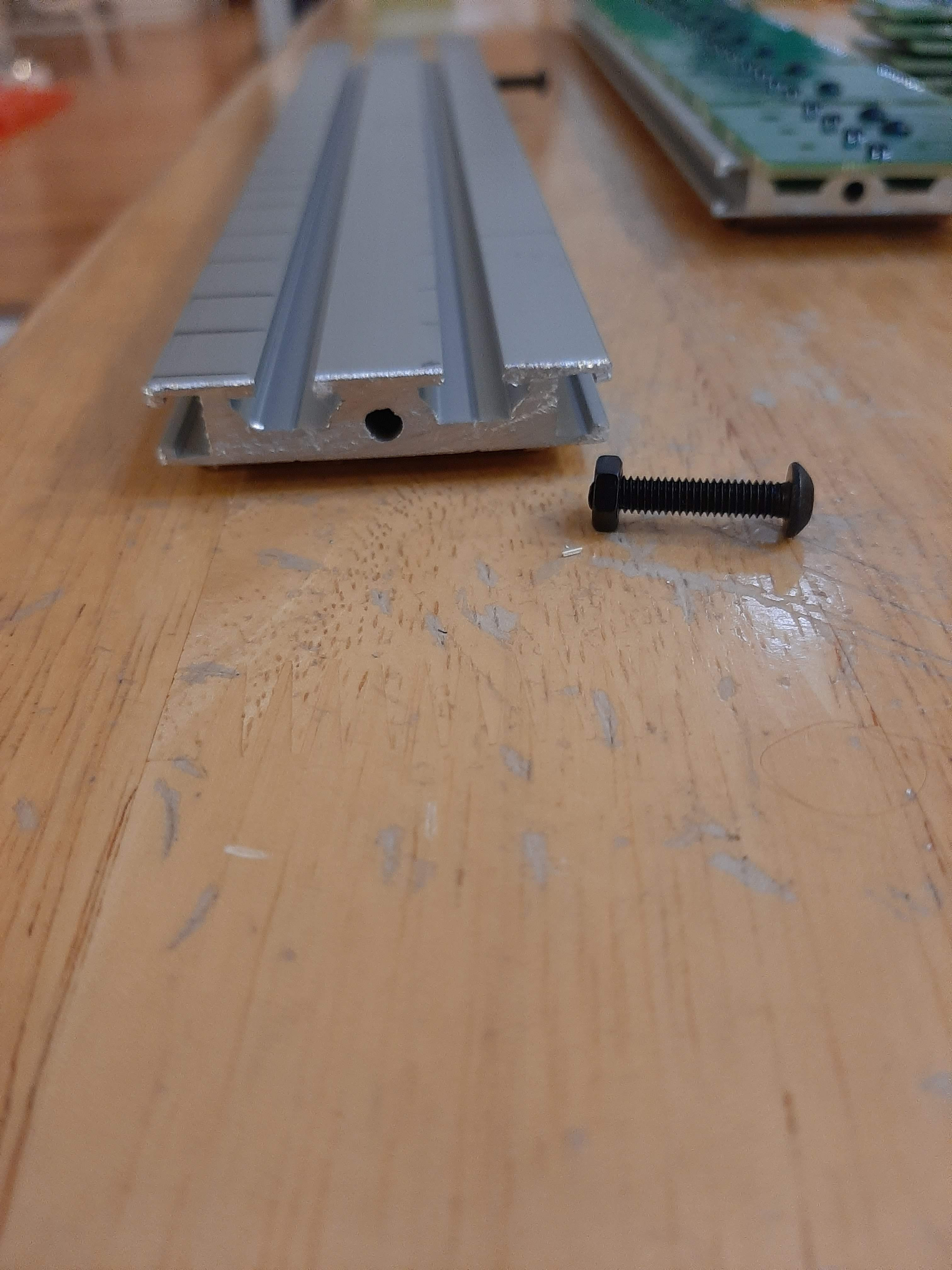
Side view. This flat extrusion conveniently has a side slot where bolts can be placed and are very nice for final attachments to the keybed.

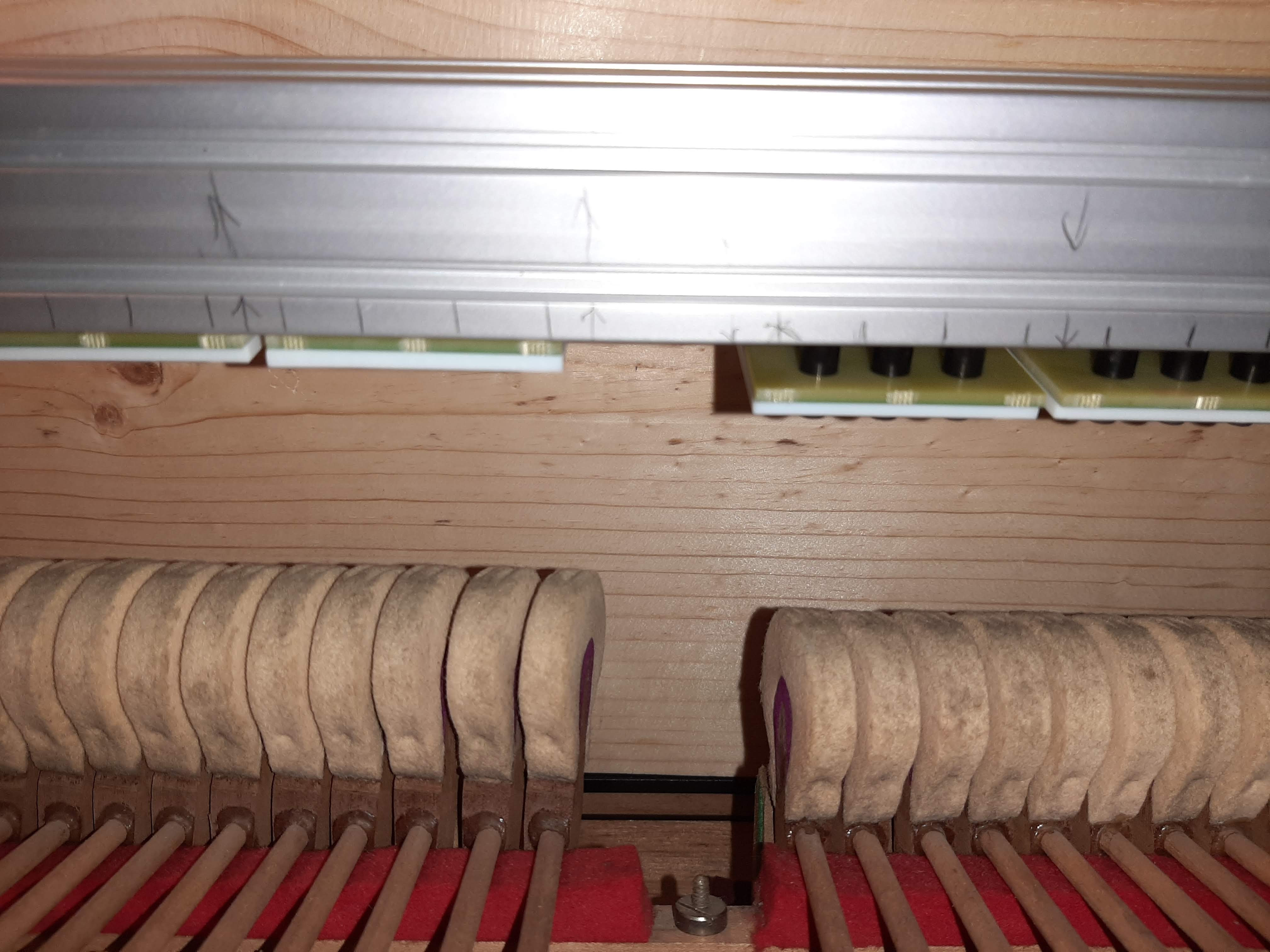
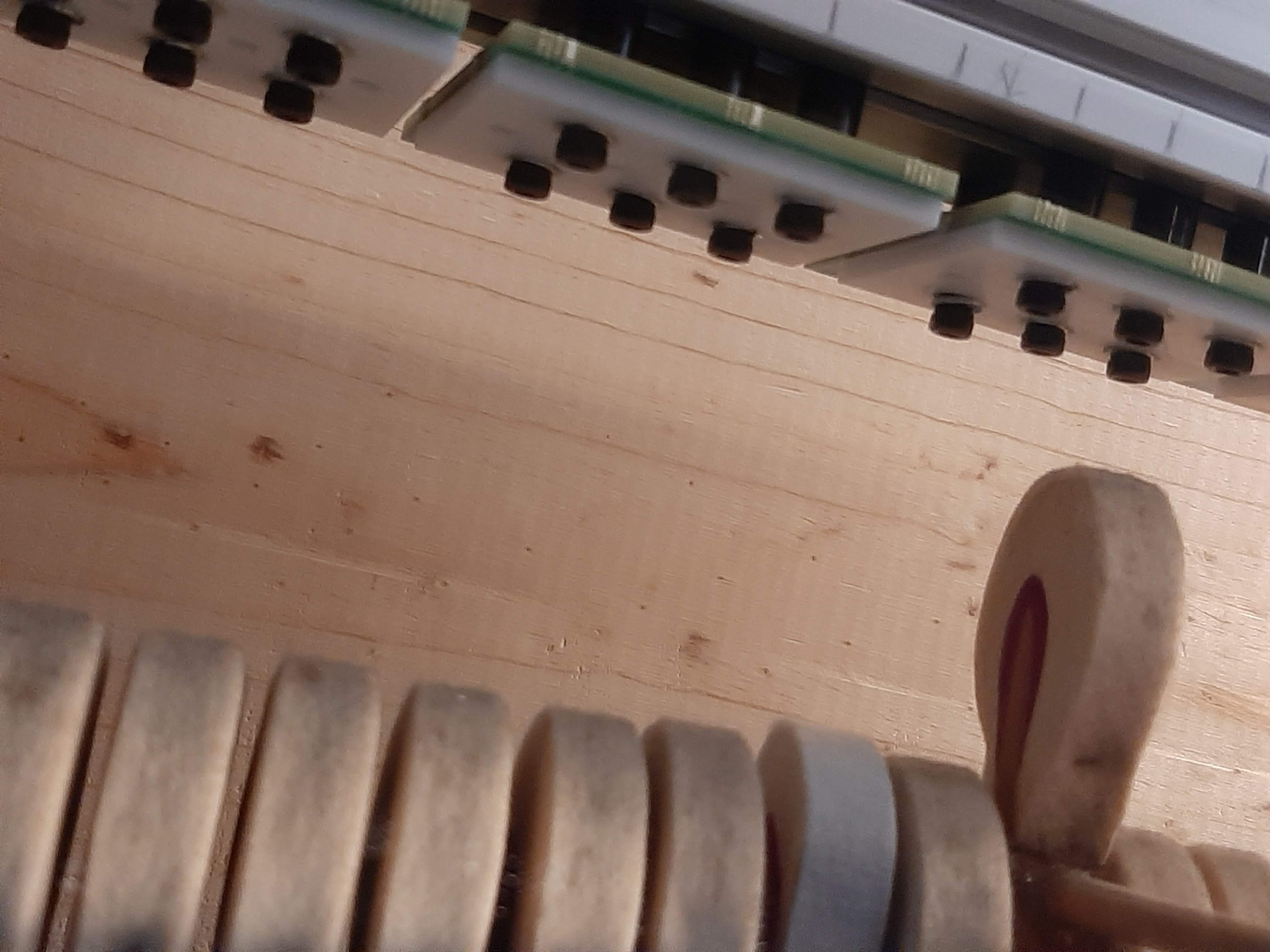
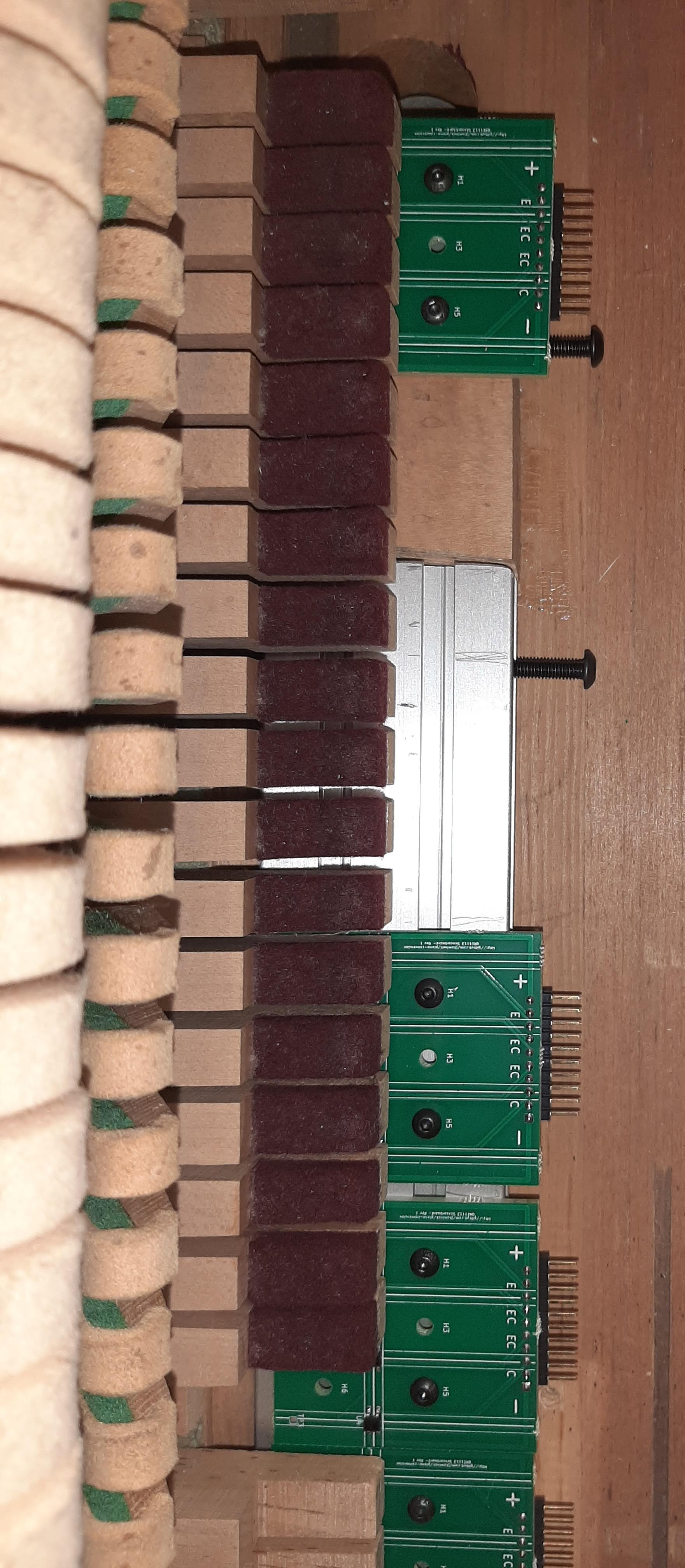
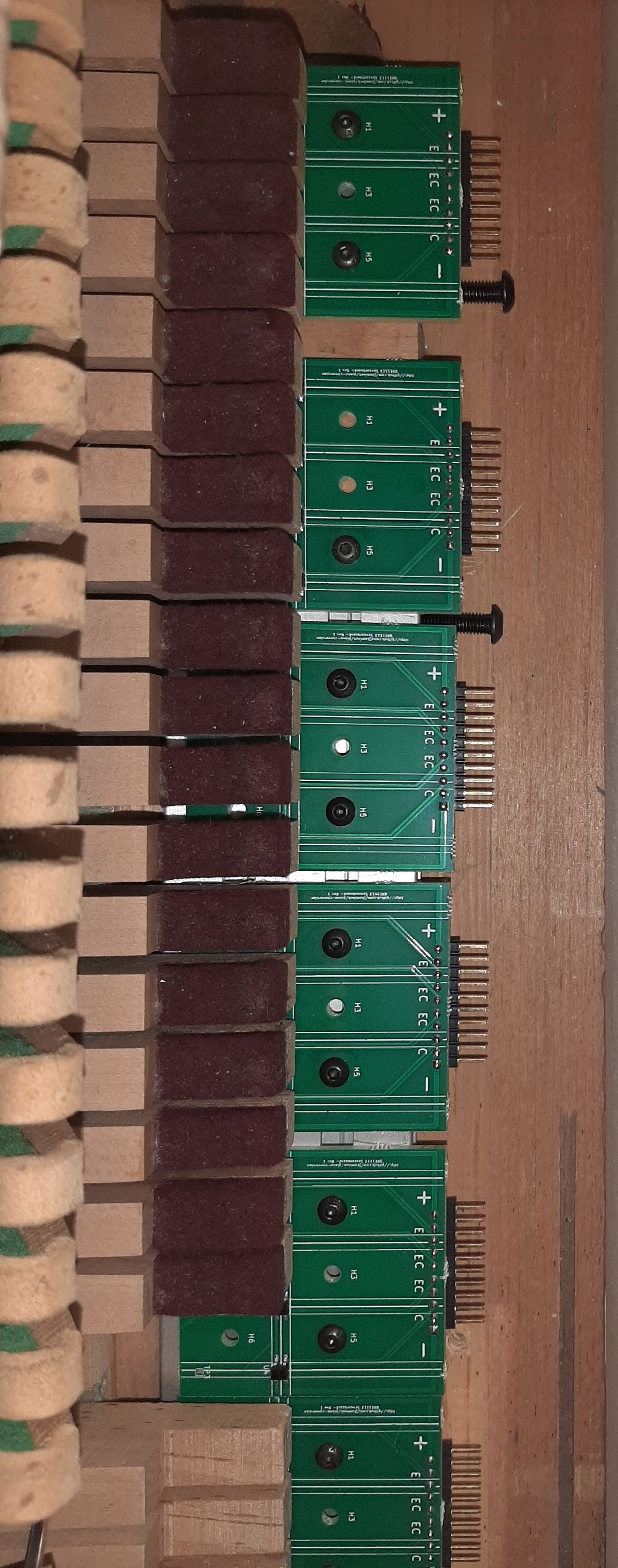
And now, in place inside the piano. Notice how convenient the silkscreen guidelines are for correct alignment, which took much less than I expected! Also notice (if you can because of perspective effects) how compromises are needed about centering the sensors in the middle of the keysticks: not always possible! It would have been a nightmare with the CNY70, and most likely I could not have done with all 4x sensorboards. Moreover, the CNY70 would have been too tick and I would have been unable to use the extrusion, so I'd have to attach the sensorboards to the keybed, making alignment even more complicated.


RIP

So, what's next?

Discussing with @JayKominek to:

  1. share my experience so far with these sensorboards (and give him a few of the spares I have in case he wants to test the manufacturing quality of the company I utilized and the pros/cons of these sensors compared to the CNY70)
  2. understand if the ADC boards and the main board designs are finalized or if what else may change

If not much would need to change with these boards, I'd move on working on a BOM for them, which will take a while (I'm glad that I started with the much simpler sensorboards!!).

The most important chips in all of them, namely STM32H743 are still affected by parts shortage, but some resellers are reporting that they have many thousands "on order", so I am hopeful (I need less than a dozen).

Meanwhile, these sensorboards will need to be connected to the ADC boards and I am working on cable design and management, as reported at https://github.com/jkominek/piano-conversion/issues/55

When I'll get at least one ADC board and at at least some preliminary cables, I'll be back in the business of making sound and if necessary writing/improving the software/firmware aspects (which as you may remember I've already done with the Raspberry Pico, but that was just proof of concept and not the "production" stage I'm now in, with infinite thanks to Mr. @JayKominek our leader)


« Previous Page